Short-range order controlled amphoteric behavior of the Si dopant in Al-rich AlGaN
Published in Materials
Prologue
The story behind this paper unfolded like a good thriller. With each new chapter, unexpected findings twisted the plot, leaving protagonists wondering on what was coming next. To unravel this mystery, we journeyed across laboratories, combining positron annihilation spectroscopy, X-ray absorption spectroscopy, and density functional theory to study the unusual behavior of a usual silicon dopant. Here is how our investigation evolved from electrical compensation in highly Si-doped AlGaN to the amphoteric behavior of Si in these alloys.
Scene of the Crime
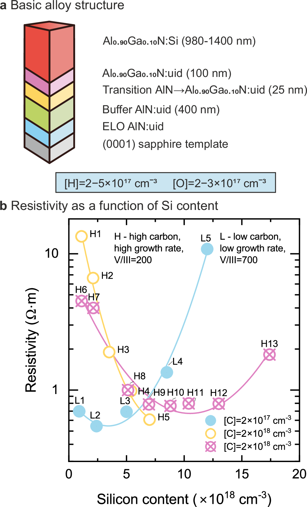
It all began with missing electrons in AlGaN thin films grown in the group of Prof. Kneissl at Technische Universität Berlin. The samples were prepared by metal-organic chemical vapor deposition with 90% aluminum mole fraction with varied V/III ratio, carbon content, and silicon doping level. The idea was straightforward: alloying GaN with AlN enables bandgap tuning, which is vital for deep-ultraviolet optoelectronics below 240 nm. And silicon, a well-known shallow donor in nitrides, was expected to enhance n-type conductivity.
The more Si, the better? Our electrical measurements told a different story as shown in Fig. 1. Resistivity initially decreased with higher [Si], as expected, until it suddenly reversed course and skyrocketed. In high-carbon samples, this turning point occurred at ~1×1019 cm⁻³ [Si]. In low-carbon samples, the shift happened even earlier, at ~5×1018 cm⁻³. Clearly, something was robbing the material of free charge carriers.
Usual Suspects
We considered the usual suspects. First, incomplete ionization. Si donors have a relatively high ionization energy in AlN, but at high [Si], enough donors should still be activated at room temperature. Second, residual acceptor impurities. But secondary ion mass spectrometry revealed that their concentrations were far lower than [Si], too low to explain the compensation.
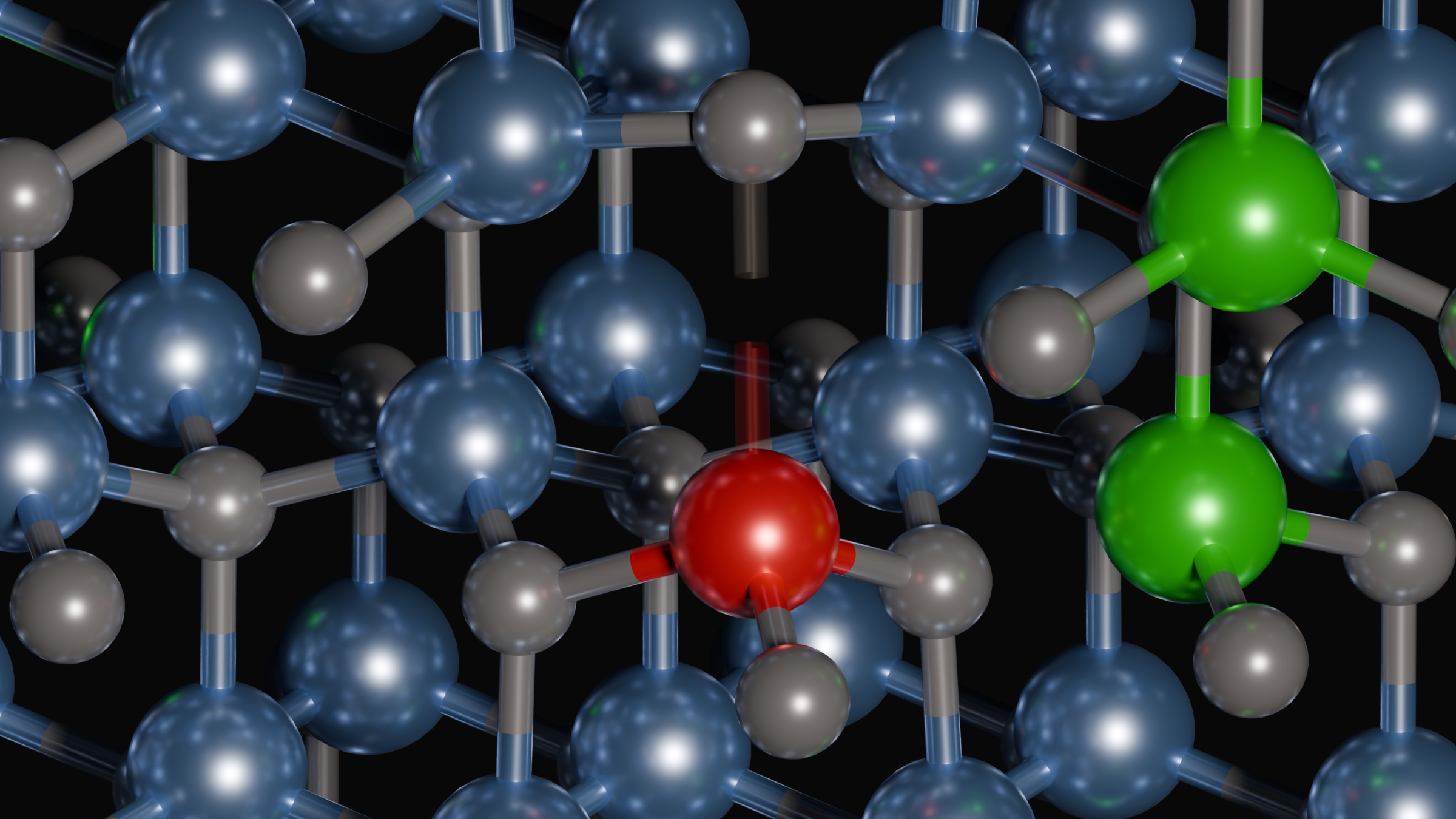
Third, cation vacancies (that is, missing Al or Ga), which tend to form in negatively charged states, especially when the Fermi level shifts toward the conduction band due to heavy n-type doping. Therefore, we probed the samples using positron annihilation spectroscopy at our positron facilities, a technique sensitive to open volume defects in the technologically important range for semiconductors of 1×10¹⁶ to 1×1019 cm⁻³.
A New Clue
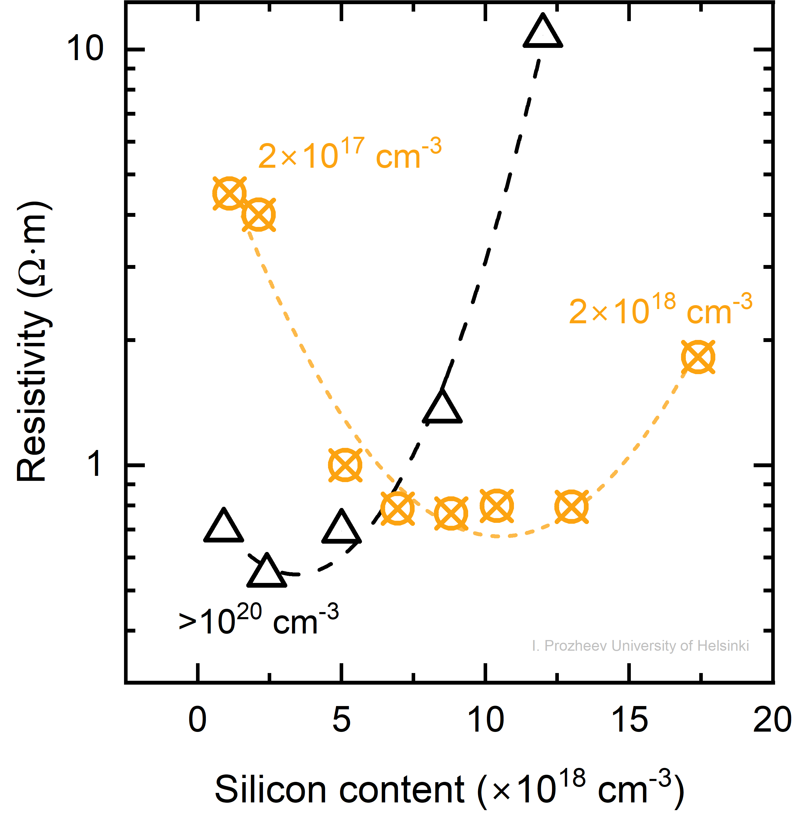
Positron experiments confirmed the presence of cation vacancies. But again, their concentrations weren’t enough to explain the dramatic rise in resistivity. In low-carbon samples, they were electrically inactive. In high-carbon samples, their concentrations combined with all other known acceptors, remained lower than [Si] in the samples where resistivity increased.
Interestingly, in two highly doped low-carbon samples, positron annihilation parameters shifted away from cation vacancies toward annihilation characteristics of the perfect AlN lattice as [Si] increased. It seemed nonsensical, until we considered the possibility of a negatively charged non-open volume defect, such as an ionized acceptor, which could still trap positrons and mimic a bulk-like signal. To test this, we repeated the measurements at elevated temperatures in selected samples that showed the data moving toward vacancy-type signals. It became clear: a hidden, negatively charged defect species was present, trapping positrons and likely compensating Si donors. By the spread in positron annihilation parameters, we estimated that this negative ion is present at concentrations comparable to [Si]. With other culprits ruled out, we focused on the least suspected: silicon itself.
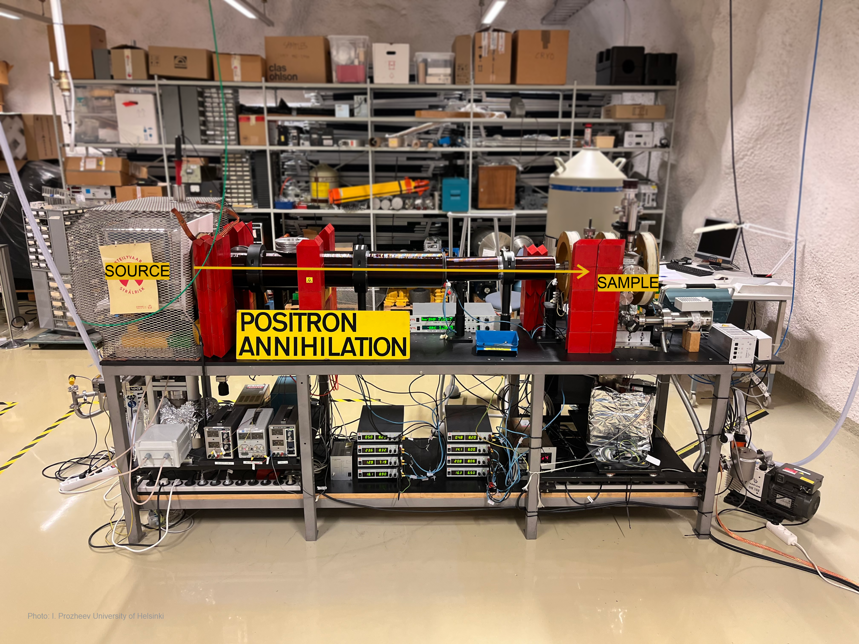
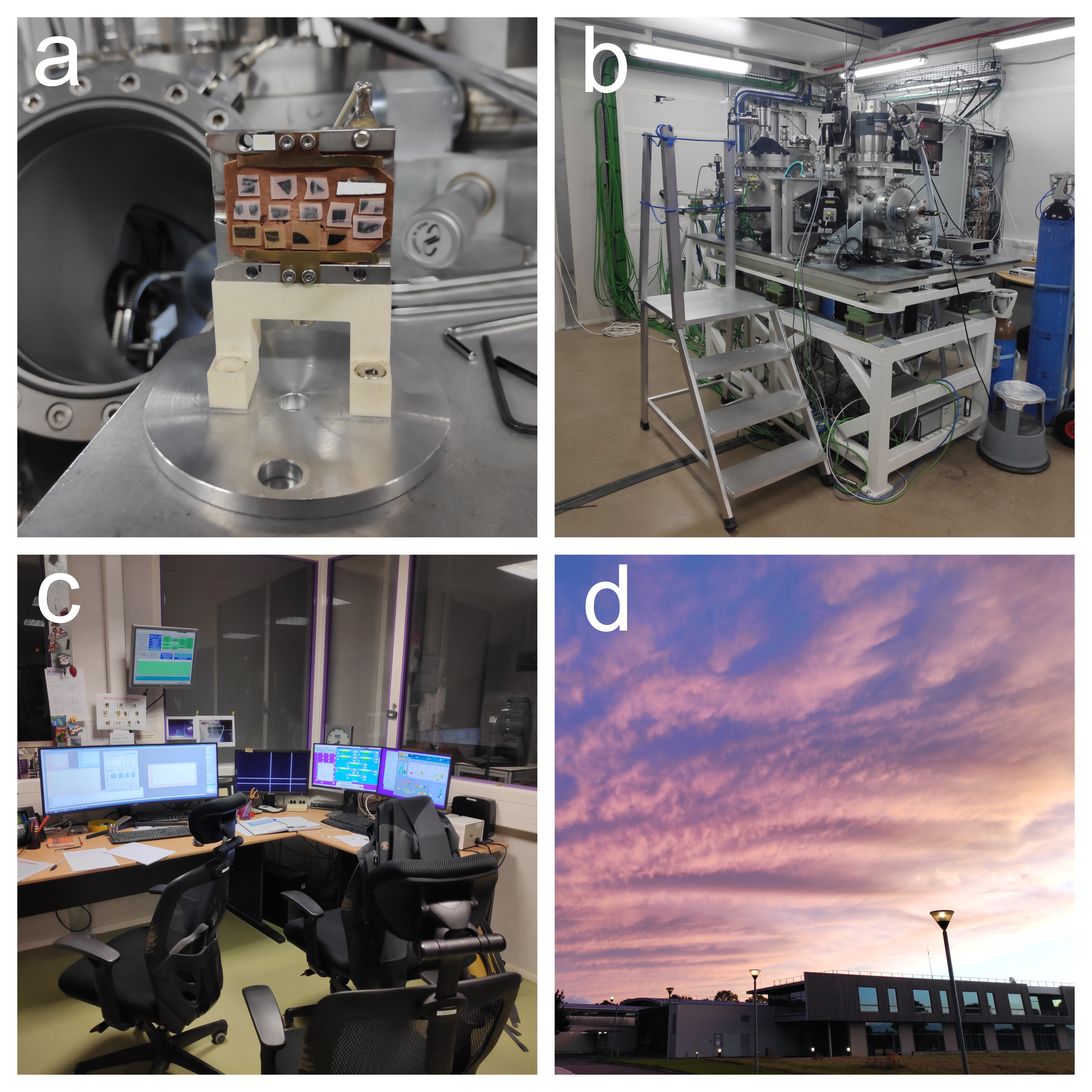
Figure 2: Slow positron beam. Positron source (inside a metal cage on the left) emits positrons that are further accelerated towards the sample chamber for the positron annihilation signals to be recorded with high purity germanium detectors.
The Breakthrough
We applied for beamtime at the LUCIA beamline at the SOLEIL synchrotron, the only facility capable of resolving the Si K-edge with soft X-rays at that time. Our goal was simple: check if any acceptor-like atoms were residing near Si that might compensate its donor activity. But the spectral fingerprints revealed something completely unexpected, as [Si] increased, the local environment of Si shifted from GaN-like to AlN-like. And this is in 90% Al random alloys!
We simulated a catalog of spectra to compare with the experimental results and found no clear sign of a mysterious impurity. Instead, we observed an overrepresentation of Ga atoms in the local lattice around Si. It seemed that with these experimental results we had the key in our hands, all we needed to find was the lock.
The Double Agent
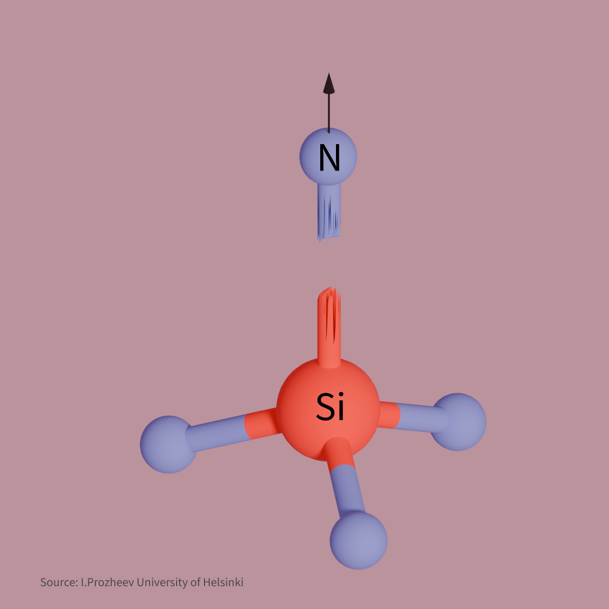
It is known that the silicon donor can form a deep DX state in AlN via strong lattice relaxation, with an acceptor level just below the conduction band edge. At high doping, the Fermi level shifts toward the conduction band, making this transition more likely. In GaN, the DX state is a degenerate level which stabilizes above the conduction band.
To test this further, we used hybrid-functional density functional theory simulations of AlGaN with various local atomic configurations around Si. The trends were striking, Si had lower formation energy in Ga-rich clusters in consistency with the local overrepresentation we had seen experimentally. However, in such clusters, the DX configuration was less likely to form. In more random, AlN-like environments, DX formation became energetically favorable.
In other words, the short-range order (the presence of excess Ga atoms around Si) directly influenced whether Si acted as a donor or turned into a compensating center. This explained the missing electrons and the resistivity increase, as Si dopants run out of available sites with enough Ga, the environment become more favorable to DX formation and compensation followed.
Epilogue
By combining advanced positron and x-ray spectroscopies and theoretical simulations, we revealed that short-range atomic order controls the amphoteric behavior of silicon in high-Al-content AlGaN. This not only solves the mystery of overcompensation at high doping levels, but also points to a way forward: intentionally tailoring the local Ga distribution could allow efficient Si doping even in AlGaN alloys with high Al molar fraction.
Whether through enhanced Ga clustering in alloys or digital superlattices with Ga-rich monolayers, we may find a way to prevent silicon from turning into a double agent and donate electrons instead of robbing them in high Al-content AlGaN alloys or even AlN.
Follow the Topic
-
Nature Communications
An open access, multidisciplinary journal dedicated to publishing high-quality research in all areas of the biological, health, physical, chemical and Earth sciences.

Related Collections
With Collections, you can get published faster and increase your visibility.
Women's Health
Publishing Model: Hybrid
Deadline: Ongoing
Biosensing
Publishing Model: Hybrid
Deadline: Sep 30, 2026


Please sign in or register for FREE
If you are a registered user on Research Communities by Springer Nature, please sign in