Stack, Shake, and Shine: NOEMS built by van der Waals heterostructures
Published in Electrical & Electronic Engineering
Significance
A fascinating nature of two-dimensional materials is that they are atomic layer thin films that can serve as nano-electro-mechanical resonators (NEMS) with characteristic frequencies above 100 MHz and often with ultrahigh quality factors at low temperatures. When taking into account optical degrees of freedom, NEMS can be expanded into nano-opto-electro-mechanical systems, known as NOEMS, a class of hybrid solid devices designed to couple optical, electrical and mechanical degrees of freedom in a nano scale.
To date, however, studies of NOEMS using van der Waals (vdW) heterostructures are very limited [1-2], although vdW materials are known for emerging phenomena such as spin, valley, and topological physics [3-5]. It thus helps to build modern sensors by exploring many emerging properties in both classical and quantum regimes.
Design and Approach
One of the major technical challenges of vdW materials based NEMS is the fabrication route itself. It is known that suspension of 2D nano sheets often undergoes solvent processes, and the surface tension induced by liquid-gas interface tears down the 2D membrane, leading to low sample yields [6-7]. It is even more difficult to obtain 2D materials based NEMS with multi-terminal configurations such as Hall bar for transverse electrical responses.

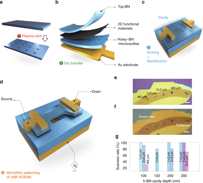
Figure 1. Optical microscopy images (a-d), and false-color scanning electron microscopy (SEM) images (e) showing a suspended vdW heterostructure. (a)-(c) Workflow of two-terminal suspended h-BN/graphene heterostructure, with a zoomed-in SEM image shown in (e). The red dashed box area in (b) and (c) shows the difference before and after plasma etching patterning of the final step of suspension. (d) A typical array of suspended vdW heterostructure Hall bar.
Here, we devise a universal method to robustly fabricate vdW heterostructures into an architecture that hosts opto-electro-mechanical couplings in one single device. In order to obtain arrays of suspended vdW heterostructures, holey h-BN was first patterned via standard lithography and plasma etching, and a dry transfer step was performed using pre-stacked few-layer vdW materials, as shown in Figure 1. Arrays of suspended vdW heterostructures were then monolithically sculpted at the final step of plasma etching. In this manner, we can obtain a high yield of suspended vdW heterostructures, without the use of a critical point drier. For example, upon a suspension height of 300 nm and a suspended area of 5 μm2, the success rate reaches 90%.
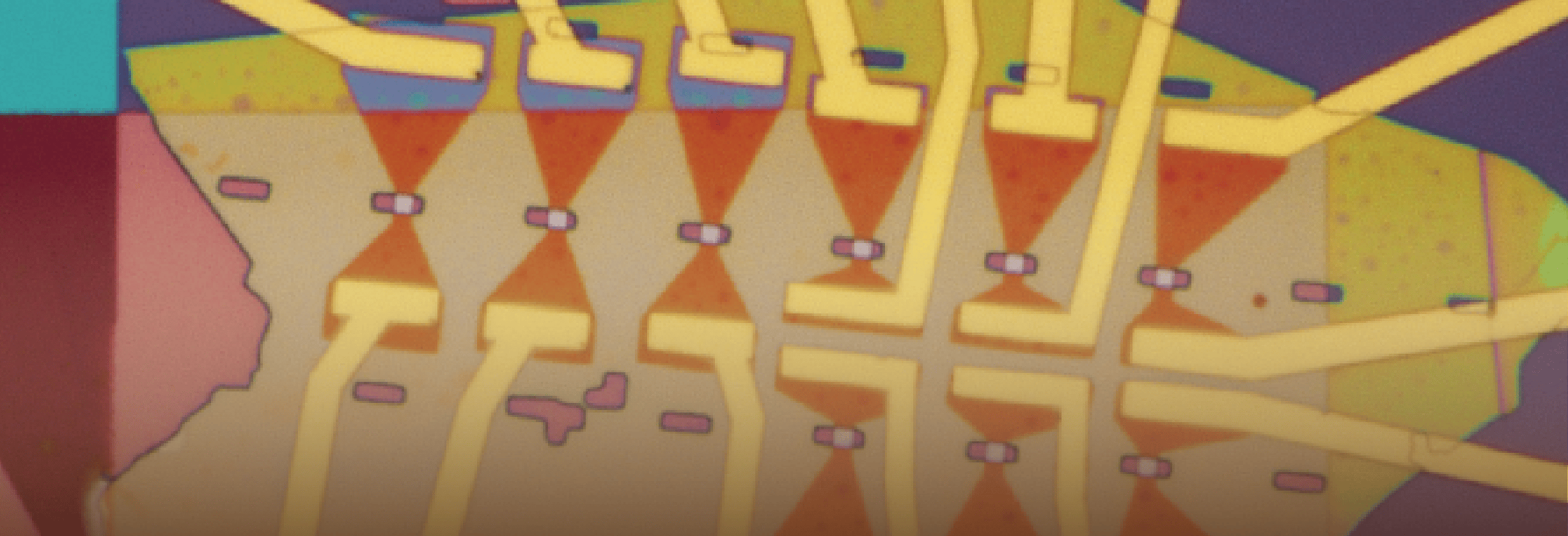
Taking h-BN/graphene heterostructure as an example, using the method described above, multi-functionalities, including nano-mechanical resonators, vacuum channel diodes, and ultra-fast thermo-radiator, can be established in a single suspended vdW heterostructure. First, when the lower surface of the suspended vdW heterostructure is set to be graphene, the whole system can serve as a vertical vacuum channel diode. Thermionic emission of electrons can be pulled out of Joule heated graphene and collected by the bottom collector electrode, with on-off ratios reaching a level up to 105 (Figure 2a-d), which remained unchanged after a total ionizing dose of 3 Mrad (Si). Second, such a typical device can be functioning at the ultra-fast regime as thermo-radiators (Figure 2e), with a wavelength of emitted light tunable by the depth of the suspension cavity. Thirdly, the resulting devices can act as nano-mechanical resonators, with resonance at the order of 0.1 GHz and quality factor reaching 1000 at room temperature (Figure 2f).

Figure 2. (a) Home-made vacuum chamber for simultaneous measurements of the optical spectrum and electrical transport in the vdW NOEMS. (b)-(c) Optical image and cartoon illustration of the device functioning as thermionic light and electron emission. (d)-(f) Thermionic electron emission diode, ultrafast thermo-radiator, and NEMS characterizations of one single device described in (c).
Perspectives
In principle, the proposed monolithically sculpted nano-opto-electromechanical vdW heterostructure system can be expanded to a wide variety of 2D materials, we can therefore select and design all kinds of vdW heterostructures based NOEMS at our needs (Figure 3a). For example, one can take advantage of the valley and spin degrees of freedom in transition metal dichalcogenides or in 2D magnetic materials to build devices with exotic opto-electro-mechanical couplings (Figure 3b-c), and can also be shaped into multi-terminal NOEMS (Figure 3d). Furthermore, their functionalities can be selectively modulated by patterning the 2D stacks into photonic crystals, which opens up opportunities for novel NEOMS (Figure 3e).

Figure 3. (a) Schematic images of 2D materials with different functionalities. (b) and (c) Cartoon of the spin and valley interactions in 2D materials. (d) False-colored SEM image of a typical multi-terminal suspension of vdW NOEMS obtained using the method described in this study. (e) Illustration of the NOEMS based on vdW heterostructures, which may be expanded into a broad range of 2D materials and their vertically stacked multilayers.
To sum up, our approach is an attempt of facile and robust fabrication protocol toward suspended vdW heterostructures (as compared, conventional suspension of 2D materials were more focused on single layers of them), as they can be a promising platform to explore many interesting properties in both classical and quantum regimes, holding promise in future applications of modern nano-sensors.
For more details, please see the original version of the manuscript in Light: Science & Applications: https://www.nature.com/articles/s41377-022-00734-7.
References
[1] Li, H.-K. et al. Valley optomechanics in a monolayer semiconductor. Nature Photonics 13, 397–401 (2019).
[2] Zhou, Y. et al. Controlling excitons in an atomically thin membrane with a mirror. Phys. Rev. Lett. 124, 027401 (2020).
[3] Zhao, S. et al. Valley manipulation in monolayer transition metal dichalcogenides and their hybrid systems: status and challenges. Reports on Progress in Physics 84, 026401 (2021).
[4] Liu, Y. et al. Van der waals heterostructures and devices. Nature Rev. Mat. 1, 16042 (2016).
[5] Dong, B., Yang, T. & Han, Z. Flattening is flattering: The revolutionizing 2D electronic systems. Chinese Physics B 29, 097307 (2020).
[6] Chen, C. et al. Performance of monolayer graphene nanomechanical resonators with electrical readout. Nature Nanotechnology 4, 861 (2009).
[7] Singh V. et al. Probing thermal expansion of graphene and modal dispersion at low-temperature using graphene nanoelectromechanical systems resonators. Nanotechnology 21, 165204 (2010).
Follow the Topic
-
Nature Nanotechnology
An interdisciplinary journal that publishes papers of the highest quality and significance in all areas of nanoscience and nanotechnology.
-
Light: Science & Applications
A peer-reviewed open access journal publishing highest-quality articles across the full spectrum of optics research. LSA promotes frontier research in all areas of optics and photonics, including basic, applied, scientific and engineering results.


Please sign in or register for FREE
If you are a registered user on Research Communities by Springer Nature, please sign in