Tailoring atomic diffusion for in situ fabrication of different heterostructures
Published in Materials
Atomic diffusion has been recognized as a particularly powerful tool for fabrication of heterogeneous nanocrystals that are not easily obtained using direct synthesis methods. However, controlled atomic diffusion is very difficult to achieve since the underlying mechanisms of this process are yet to be fully revealed, principally due to the lack of direct and real-time observations.
Nowadays, the in situ transmission electron microscopy (TEM), which can be introduced several different external fields, brings us a chance to visualize the controlled atomic diffusion reactions at nanoscale. We set up a series of in situ tailored atomic diffusion experiments inside a TEM by applying a voltage bias (Fig. 1a). Using this method, it is possible to efficiently control atom diffusion to selectively fabricate either a core-shell nanostructure or a segmented binary heterostructure in the Ag-Te nanowire system. Under the application of positive bias with a direction of Ag nanowire to Te nanowire for a few minutes, a significant number of Te atoms diffuse to the Ag nanowire and eventually form an Ag2Te-Ag core-shell structure (Fig. 1b). In contrast, a Ag2Te-Te binary heterostructure is formed ultimately when the applied electrical field is Ag to Te (Fig. 1c).
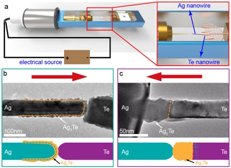
Fig. 1. The tailored atomic diffusion experiments for fabrication of different heterostructures by applying a bias inside a TEM. a, Schematic illumination of the setup for tailored atomic diffusion experiments. b, The formation of the Ag2Te-Ag core-shell structure by applying a positive voltage; the structure of the core-shell nanowire is illustrated at the bottom. c, TEM image and the illustration showing the formation of Ag2Te-Te binary heterostructure when applying a negative voltage (red arrows showing the direction of current).
When a bias is applied to the material system, collisions between the conduction electrons and the atoms can lead to the diffusion of the atoms, which is the diving force for directional diffusion in these experiments. When a positive voltage with the direction of Ag to Te is applied to the Ag-Te system, Te atoms diffuse to Ag nanowire along the surface under the influence of electron-wind force, and then the diffused Te atoms react with Ag to form Ag2Te crystallite. Small pieces of Ag2Te islands are connected into sheets, and finally, a shell layer is formed on the surface of the Ag nanowire (Fig. 2a-f). In contrast, Ag atoms begin to diffuse into Te crystal by the path of bulk diffusion under a negative voltage bias. Te atoms and the migrated Ag atoms will undergo a process of phase transformation to form Ag2Te when the atomic ratio is appropriate. Finally, the Te nanowire becomes the Ag2Te-Te binary heterostructure (Fig. 2g-l).
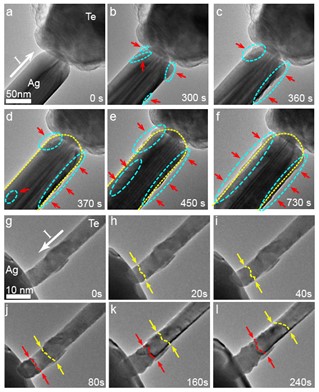
Fig. 2 The formation of different heterostructures when the direction of bias changes. a–f, TEM image series showing the formation of an Ag2Te-Ag core-shell structure when 0.3 V bias was applied to the system. The red arrows and blue dashed circles indicate the growth of the Ag2Te crystallite or shell, whereas the yellow dotted lines trace the shape of the Ag nanowire before biasing. g-l, TEM image series showing the growth of Ag2Te under −0.8 V bias applied. The yellow dashed lines highlight the diffusion frontier, and the red dashed lines indicate the phase transformation frontier.
The diffusion path can strongly affect the final morphology of the as-formed heterostructures. Generally, surface diffusion takes priority over bulk diffusion in the solid materials owing to the lower diffusion barrier, however, bulk diffusion can be comparable if the system temperature is high enough when the thermal energy could help more atoms or ions to conquer the barrier of bulk diffusion. A model was constructed to probe the temperature distribution of the Ag-Te system under a bias. In consideration of the large difference of thermal conductivity between Ag (429 Wm−1K−1) and Te (2.35 Wm−1K−1), the side of Te nanowire will show a much higher and slowly changing temperature while the temperature reduces to the room temperature in a very short distance in Ag nanowire (Fig. 3a). Once the Ag atoms diffuse into Te nanowire under a negative bias, the large thermal energy on the Te side could be enough for Ag atoms to conquer the barrier of bulk diffusion in Te. Consequently, bulk diffusion is substantial for Ag atoms in Te nanowire, resulting in binary hetero-structured nanowire (Fig. 3b). In contrast, for the diffused Te atoms in Ag nanowire, surface diffusion still dominates over bulk diffusion due to the low temperature, resulting in the core-shell structure (Fig. 3c).
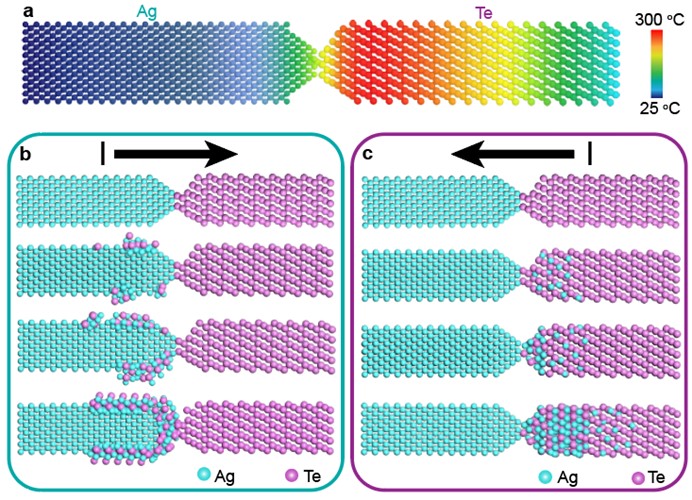
Fig.3 Formation mechanism of Ag-Te heterostructures. a, Schematic image showing the temperature distribution in the Ag-Te system. b, c, Schematic diagrams showing the formation process of Ag2Te-Ag core-shell structure and Ag2Te-Te axial segmented heterostructure.
Our results provide a new perspective to synthesis individual nanostructures with an electrically driven atomic diffusion reaction and throw light on the micro-mechanism of solid–solid processes.
For more details, please check out our paper “Tailoring atomic diffusion for in situ fabrication of different heterostructures” in Nature Communications.
Link: https://www.nature.com/articles/s41467-021-25194-2
Follow the Topic
-
Nature Communications
An open access, multidisciplinary journal dedicated to publishing high-quality research in all areas of the biological, health, physical, chemical and Earth sciences.
Related Collections
With Collections, you can get published faster and increase your visibility.
Women's Health
Publishing Model: Hybrid
Deadline: Ongoing
Biosensing
Publishing Model: Hybrid
Deadline: Jun 30, 2026



Please sign in or register for FREE
If you are a registered user on Research Communities by Springer Nature, please sign in