Templated dewetting of single-crystal sub-millimeter-long nanowires and on-chip silicon circuits
Published in Electrical & Electronic Engineering
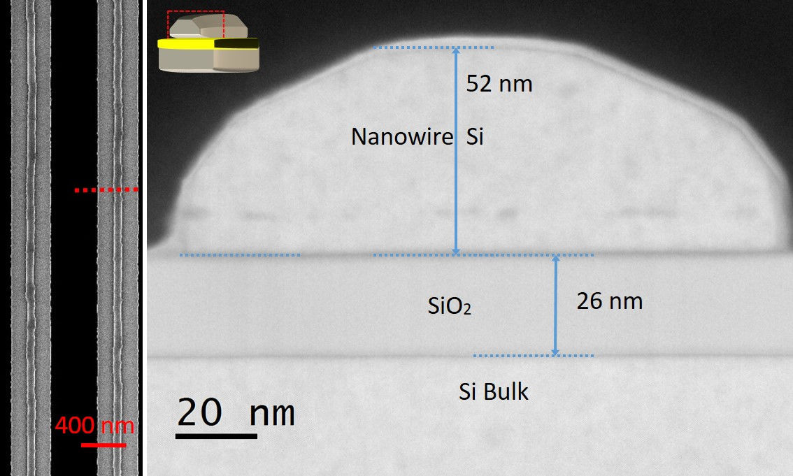
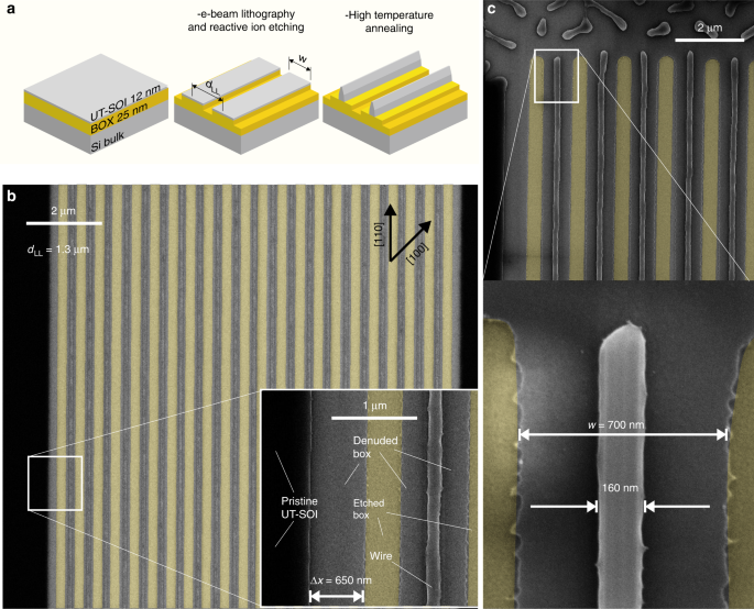
Large-scale, defect-free, micro- and nano semiconductor circuits with controlled inter-connections represent the nexus between electronic and photonic components. Semiconductor nanowires exhibit superior and configurable electronic and optical properties. Their disruptive potential has been demonstrated in photonics (e.g., for lasers or quantum optics), electronics, thermoelectricity, energy storage with batteries, gas and mechanical sensing, topological quantum states and much more. For these reasons, their growth has been tackled with a plethora of techniques aiming at the production of controlled, ultra-long structures matching the needs of high yield, scalability (e.g., integration of a large number of devices on the same monolithic nano-wire) and material quality (e.g., smooth interfaces). As such, the range of available approaches to growing elongated crystalline structures steadily increases, from direct top-down design, as, e.g., three-dimensional mesoscale lithography, superlattice nanowire pattern transfer up to the exploitation of natural phenomena such as the renowned Plateau-Rayleigh instability. Several bottom-up, self-assembly methods can be employed to obtain high-quality parallel wires. Nevertheless, full control over their morphology, size, position, direction, inter-connection, and electrical isolation remains a challenge as current techniques are not versatile and are limited to a few micrometers length. On the other side, top-down lithographic methods can be used to precisely prepare a substrate for further engineering, as for instance shown for the cases of controlled wetting or nano-imprint lithography. However, their exploitation in scalable devices is often hindered by the complexity of their implementation requiring too many, cumbersome nano-fabrication steps. In fact, these approaches often need high-resolution etching and provide out-of-plane objects, eventually requiring further processing before their implementation in a device. In this work, we show an original fabrication method for the implementation of ~mm long Si-based nanowires and complex circuits of connected wires. We exploit solid-state dewetting (a natural instability of thin solid films) to precisely and independently control the size, position, direction and inter-connections of mono-crystalline (atomically smooth, faceted) wires on insulator. The control of this templated dewetting process is extended to silicon patches having the record aspect ratio of 1/60000. We benchmark these results against theoretical simulations (phase-field simulations), showing clarifying the role of the crystal anisotropy in stabilizing the wires against breaking. Moreover, as a practical application, we use our wires as a platform for transistors exploiting a simple spin-on-dopant process after dewetting and contact deposition. The importance of the demonstration of a transistor on this platform relies on the size of these structures that perfectly meet the needs for dielectric nanoantennas working at visible and near-infrared frequencies. Thus our technique is a step forward towards an efficient integration of electronic and photonic devices on the same silicon-based platform.
Follow the Topic
-
Nature Communications
An open access, multidisciplinary journal dedicated to publishing high-quality research in all areas of the biological, health, physical, chemical and Earth sciences.

Related Collections
With Collections, you can get published faster and increase your visibility.
Women's Health
Publishing Model: Hybrid
Deadline: Ongoing
Biosensing
Publishing Model: Hybrid
Deadline: Sep 30, 2026


Please sign in or register for FREE
If you are a registered user on Research Communities by Springer Nature, please sign in