The Reciprocal Evolution of AI and Computer Architecture: Bridging the Moore’s Law Gap with Network-on-Chip (NoC) and Machine Learning
Published in Protocols & Methods, Computational Sciences, and Mathematics


The End of Moore’s Law: What’s Next?
For decades, Moore’s Law has driven the exponential growth of computing power. However, as we hit the physical limits of silicon, it becomes increasingly challenging to sustain this pace. This raises a critical question: How can we continue advancing computing capabilities when Moore's Law is no longer viable?
Here’s where AI and ML offer a transformative opportunity. These technologies not only require more powerful architectures to function, but they also offer solutions to make those architectures more efficient. This reciprocal relationship between AI, ML, and computer architecture is reshaping how we approach the future of technology.
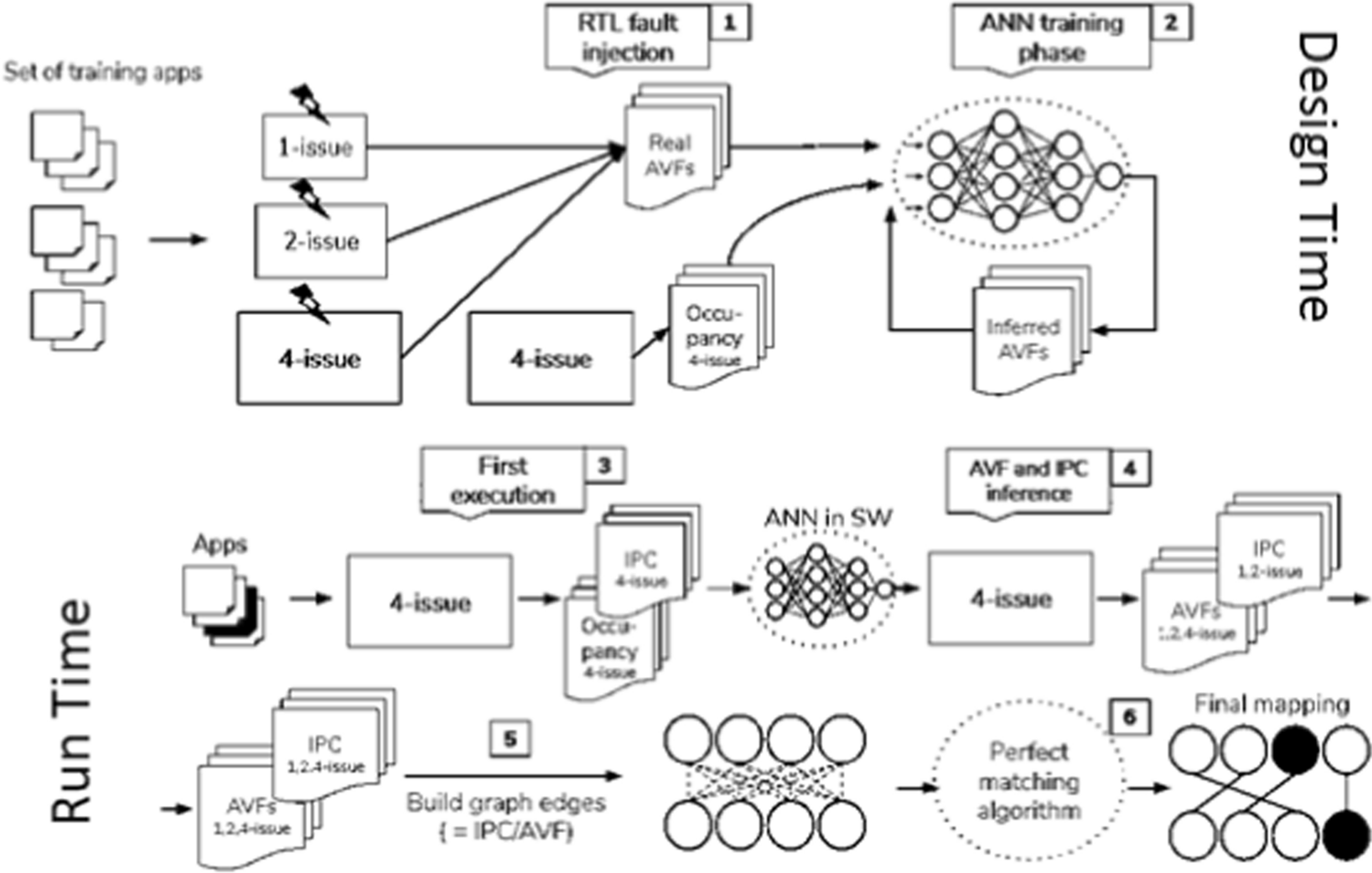
What is Application Mapping?
At its core, application mapping is the process of assigning tasks or workloads (like specific computations or data processes) to various components within a computing system—such as processors, memory units, or communication links. Think of it like organizing a team project where you need to decide who does what based on their strengths and resources.
In the context of Network-on-Chip (NoC) technology, application mapping involves strategically distributing these tasks across different cores in a multi-core chip. The goal is to optimize performance, reduce communication delays, and enhance overall efficiency.
For example, if you have a computing task that requires heavy data processing, you would want to assign it to a core that has the best capability for handling such a load. At the same time, you need to consider how these cores communicate with each other to ensure that data flows smoothly without bottlenecks.
By effectively mapping applications to the available resources, we can improve how the chip operates, making it faster and more efficient—essential in meeting the rising demands of AI and machine learning applications.
AI and Computer Architecture: A Symbiotic Relationship
AI and ML are pushing the limits of current hardware, demanding greater computational power, efficiency, and scalability. At the same time, machine learning techniques can help optimize the hardware itself. This symbiotic relationship holds the potential to make unprecedented advancements in both fields.
My recent work, A Comprehensive Study and Holistic Review of Empowering Network-on-Chip Application Mapping through Machine Learning Techniques, delves into how ML techniques—including supervised learning, reinforcement learning, and neural networks—can be used to optimize NoC application mapping. These methods enable more efficient and adaptable on-chip communication architectures.
For instance, supervised learning methods, such as artificial neural networks (ANNs), can improve core vulnerability prediction and runtime mapping. Additionally, reinforcement learning (RL) approaches, including actor-critic frameworks, can reduce communication costs and power consumption by learning to adapt to changing workloads dynamically.
Machine Learning in NoC Mapping: Challenges and Future Directions
The field of applying ML to NoC mapping is still relatively new, but it is expected to grow rapidly as NoC complexity increases. ML offers one of the most promising approaches to address the mapping challenges in NoCs, which is crucial for optimizing on-chip communication.
In my study, I explore key challenges and future research directions that are vital for unlocking the full potential of ML-driven NoC mapping. These include:
Scalability: As NoC architectures become larger and more complex, ML algorithms need to scale effectively. Future research could focus on developing scalable ML models and techniques such as distributed training, model quantization, and hardware acceleration to make ML more practical for large-scale NoCs.
Data Dependence: High-quality datasets are crucial for training ML models. Building comprehensive, representative datasets that encompass a wide range of workloads and system conditions is essential for optimizing NoC mapping. Researchers could focus on benchmark datasets, data generation techniques, and collaborative efforts between academia and industry.
Adaptation to Emerging Technologies: NoC architectures are constantly evolving with new advancements like 3D integration and optical interconnects. ML models must adapt to these technological changes, and ongoing research will be required to integrate ML into emerging NoC design paradigms.
Power Efficiency: Power consumption and thermal management are critical concerns in modern computing systems. ML techniques could help optimize both performance and power efficiency. Developing models that balance these conflicting objectives, while avoiding thermal hotspots, is a promising research direction.
Real-time Decision-Making: Low-latency decision-making is essential for real-time NoC applications. Future studies should focus on reducing computational overhead through model simplification, hardware acceleration, and efficient parallelization to ensure that ML models can make quick, accurate mapping decisions.
Interpretability: Many ML models, especially deep learning approaches, are seen as black boxes, which makes it difficult to explain their decision-making processes. Ensuring transparency and robustness in ML-based NoC mapping is vital for practical adoption. Future research could explore techniques for developing interpretable ML models.
These challenges and directions offer an exciting roadmap for researchers to explore. The integration of ML into NoC mapping will not only enhance the efficiency of communication architectures but also create opportunities for sustainable computing systems.
How This Work Contributes to the Field
My paper aims to shed light on these challenges while offering potential solutions. For instance, reinforcement learning-based strategies can dynamically manage resource allocation and reduce communication costs. Similarly, techniques like Graph Neural Networks (GNNs) improve fault detection and robustness in NoC architectures, ensuring reliable communication even in complex environments.
By analyzing various ML techniques, my work highlights the potential to optimize communication costs, power consumption, and fault tolerance in NoC systems. However, I also acknowledge the challenges, such as the computational overhead of real-time ML models, the dependency on high-quality datasets, and the difficulty in scaling ML solutions for larger NoCs.
The ultimate goal is to enable dynamic and intelligent mapping strategies that adjust to varying workloads and optimize performance. These advances represent a significant step forward in addressing the complexity of modern computing systems.
A Step Toward the Future
In 1959, the visionary physicist Richard P. Feynman, in his famous talk, proclaimed, “There is plenty of room at the bottom.”
He predicted that we would one day manipulate materials at the atomic level, creating more precise and controlled structures. This profound insight highlighted the vast possibilities for advancement in science and technology as we zoom in on the minute details that form the foundation of our creations.
Now, as we navigate the rapidly evolving landscape of artificial intelligence (AI) and machine learning (ML), we can confidently assert that there is indeed much more room for advancement at the foundational levels of these technologies. Just as Feynman envisioned building upwards from the atomic scale, we can explore the infinite possibilities that AI and ML offer by focusing on the smaller, foundational aspects of these fields.
This perspective encourages us to shift our attention from the limitations of what we cannot achieve to the incredible potential of what we can accomplish within the realms of AI and ML. The depth of opportunity in these fields is vast, and the potential for innovation is boundless.
The future of NoC application mapping lies in the collaboration between AI, ML, and computer architecture. By addressing current challenges and advancing research in key areas, researchers can unlock the full potential of ML-driven architectures. My study emphasizes that while traditional methods have provided a solid foundation, ML techniques represent a leap forward in optimizing on-chip communication.
As the complexity of NoC architectures grows, ML algorithms must evolve in parallel, becoming more scalable, efficient, and adaptable. For researchers, this paper offers a comprehensive review of the state of the field, highlights key areas for innovation, and encourages a collaborative effort between academia and industry to solve the pressing issues in NoC design.
Final Thoughts
As we move beyond Moore’s Law, the reciprocal relationship between AI, ML, and computer architecture becomes increasingly crucial. These fields must evolve together to ensure that future computing systems are more efficient, resilient, and adaptable.
This paper is a small step toward solving these complex challenges, but the potential for AI-optimized architectures is vast. By addressing the current limitations and focusing on future research directions, we can push the boundaries of NoC design and unlock a new era of high-performance computing systems.
You can read this paper here completely:
https://link.springer.com/article/10.1007/s44291-024-00027-w
I am a dedicated Researcher, Computer Engineer, Lecturer, and Reviewer, specializing in cutting-edge technologies such as Machine Learning, Artificial Intelligence, and Data Science.
In my research endeavors, I focus on developing advanced algorithms and models that drive innovation in Machine Learning and Data Science. I am particularly interested in exploring the intersection of Computer Engineering and AI, seeking applications that offer impactful solutions across various domains.
As an enthusiastic educator, I am committed to teaching and mentoring students in the fields of Machine Learning, Artificial Intelligence, and Data Science. My goal is to equip them with the skills necessary to excel in these rapidly evolving areas.
Follow the Topic
-
Discover Electronics
This is a fully open access, peer-reviewed journal that supports multidisciplinary research and policy developments across the fields of electronics and electrical engineering.

Related Collections
With Collections, you can get published faster and increase your visibility.
2D Materials for Advanced Electronics: Functional Properties, Device Integration, and Emerging Applications
This collection aims to highlight recent advances in the discovery, design, and functionalization of two-dimensional (2D) materials, including transition metal chalcogenides (TMCs), MXenes, phosphorene, their heterostructures, and quantum dots, for next-generation electronic, optoelectronic, and sensing systems.
We welcome contributions exploring theoretical, computational, and experimental investigations into the electronic, magnetic, optical, and thermal properties of 2D materials, with a strong emphasis on their integration into functional devices and engineered systems. Studies that leverage advanced spectroscopic techniques or first-principles modeling are especially encouraged, given their relevance to understanding structure–property relationships in both organic–inorganic hybrid systems and low-dimensional quantum materials.
Topics of interest include, but are not limited to:
- Data-driven and AI-assisted materials discovery and design
- Optoelectronic characterization and photonic behavior
- Synthesis and fabrication techniques tailored for device applications
- 2D materials in flexible electronics, bioelectronics, and quantum devices
- Electronic and optical sensors
- Nanostructures and hybrid systems for energy-efficient applications
This collection seeks to bridge fundamental materials research with practical applications in areas such as microelectronics, quantum electronics, circuit integration, and electronic materials—supporting the broader advancement of systems engineering, instrumentation, and applied electronic technologies.
This Collection supports and amplifies research related to SDG 9.
Keywords: 2D materials; MXenes; Transition metal chalcogenides (TMCs); Phosphorene; Quantum dots; Electronic materials; Data-driven material discovery; Device integration; Optoelectronic devices; Sensors and sensing systems; Functional electronic systems
Publishing Model: Open Access
Deadline: Oct 30, 2026
Advanced Microwave and Antenna Technologies for Next-Generation Wireless
Advanced Microwave and Antenna Technologies for Next-Generation Wireless The rapid evolution of wireless communication—driven by 5G, emerging 6G concepts, advanced radar systems, and the expanding Internet of Things—has created unprecedented demand for high-performance microwave and antenna solutions. This Collection aims to highlight recent advancements, design innovations, and emerging technologies that enable efficient, reliable, and scalable high-frequency electronic systems. We welcome original research and review articles addressing the design, analysis, fabrication, and application of microwave components, antenna systems, and electromagnetic structures that support next-generation wireless networks. Submissions may explore novel materials, miniaturized and integrated designs, reconfigurable and intelligent antenna architectures, high-frequency circuit technologies, and computational or AI-assisted optimization techniques. Studies focusing on mmWave, sub-THz, and wideband solutions for communication, sensing, and radar applications are especially encouraged. This Collection seeks to bring together contributions from academia, industry, and research laboratories to advance the state of the art in wireless hardware design. By showcasing interdisciplinary approaches and emerging trends, the Collection aims to accelerate innovation across microwave engineering, antenna design, and applied electromagnetics, supporting the continued development of future wireless systems.
This Collection supports and amplifies research related to SDG 9.
Keywords: AI-assisted RF design; 6G Antenna Design; Microwave engineering; Reconfigurable and tunable antennas; Metamaterials and metasurfaces; Radar Systems; Wireless Communication; MmWave/THz
Publishing Model: Open Access
Deadline: Sep 08, 2026


Please sign in or register for FREE
If you are a registered user on Research Communities by Springer Nature, please sign in