Two-plasmon spontaneous emission from a degenerately-doped nonlocal epsilon-near-zero material
Published in Electrical & Electronic Engineering

Plasmonics is a vibrant field of research exploiting the light-matter interaction in metallic nanostructures. Plasmonic cavities can provide deep subwavelength light confinement, opening up new avenues for enhancing the spontaneous emission process towards both classical and quantum optical applications. Conventionally, light cannot be directly emitted from the plasmonic metal itself, remaining a grand challenge to generate single- or entangled-surface plasmon polaritons (SPPs) directly from the plasmonic metal.
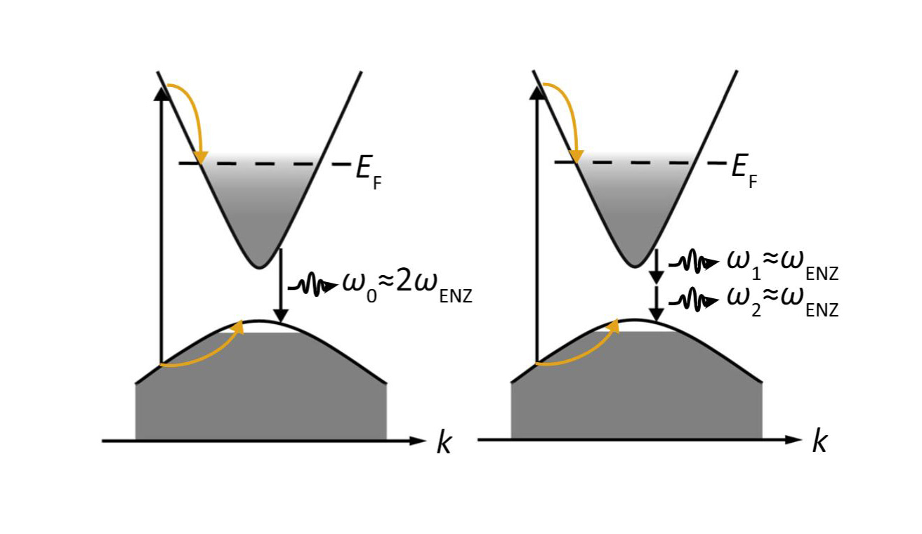
Two-photon emission (TPE) refers to the simultaneous emission of two photons during a radiative transition process. Recent researches suggest TPE rate may be selectively enhanced by the Purcell effect, as a promising approach to generate entangled photon pairs in semiconductors (for it emits two photons with intrinsic energy conservation and time concurrence) [1, 2]. Here, researchers propose a scheme to achieve efficient two-plasmon spontaneous emission (2PSE), by employing a degenerately doped semiconductor ENZ thin film that simultaneously serves as the light-emitting medium and the plasmonic cavity, as illustrated in Fig. 1. The proposed structure consists of a 50-nm-thick degenerately doped InSb film sandwiched between two AlSb layers, which are known to support SPP modes in the mid- and far-infrared.

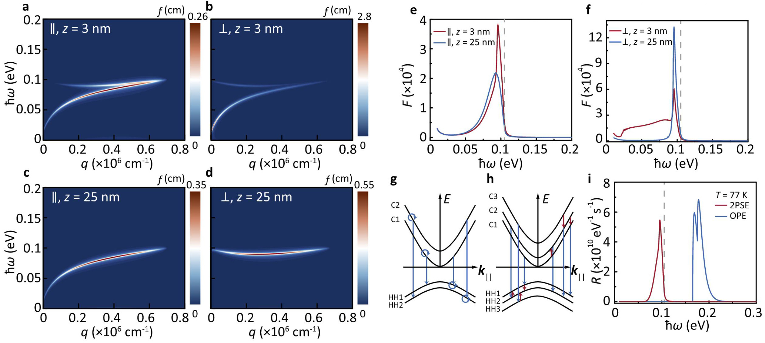
The performance of the resultant devices are summarized as Fig. 2 (see the original article & its supplementary info & for details). In conclusion, ultrafast and tunable 2PSE is theoretically shown to be potentially realized in a nonlocal ENZ film [3, 4], by spatially and spectrally matching 2PSE with highly confined SPP modes. Similar concepts can be extended to other semiconductors, 2D materials, and superconductors supporting Josephson plasmons. The 2PSE lifetime could be reduced from tens of milliseconds to several nanoseconds, comparable to the one-photon emission rate. Furthermore, we show that the optical nonlocality may largely govern the optical response of the ultrathin ENZ film. Efficient 2PSE from a doped semiconductor film may provide a pathway towards on-chip entangled light sources, with an emission wavelength and bandwidth widely tunable in the mid-infrared.

References:
[1] Rivera, N. et al. Shrinking light to allow forbidden transitions on the atomic scale. Science 353, 263–269 (2016).
[2] Goncalves, P. et al. Plasmon–emitter interactions at the nanoscale. Nature Communications 11, 366 (2020).
[3] Hu, F. et al. High-contrast optical switching using an epsilon-near-zero material coupled to a Bragg microcavity. Optics Express 27, 26405 (2019).
[4] Yang, Y. et al. High-harmonic generation from an epsilon-near-zero material. Nature Physics 15, 1022–1026 (2019).
Article info:
Two-plasmon spontaneous emission from a nonlocal epsilon-near-zero material, Communications Physics, 4, 84 (2021).
DOI: 10.1038/s42005-021-00586-4
Link: https://www.nature.com/articles/s42005-021-00586-4
Follow the Topic
-
Communications Physics
An open access journal from Nature Portfolio publishing high-quality research, reviews and commentary in all areas of the physical sciences.
Related Collections
With Collections, you can get published faster and increase your visibility.
Relativistic Astrophysical Plasmas in space and the lab
Publishing Model: Open Access
Deadline: Jun 30, 2026
Physics-Informed Machine Learning
Publishing Model: Hybrid
Deadline: May 31, 2026


Please sign in or register for FREE
If you are a registered user on Research Communities by Springer Nature, please sign in