A device bridging laboratory-scale measurements and potential near-field radiative heat transfer applications in energy conversion and thermal management
Published in Electrical & Electronic Engineering

Imagine trying to maintain a gap spacing of 10 cm between two, 5 by 5 km2 surfaces. This is obviously a very challenging endeavour. Now, if we scale down the problem to 5 by 5 mm2 surfaces, the corresponding gap spacing becomes 100 nm, which is roughly 1000 times smaller than the diameter of a human hair. This scaled down problem is not easier to solve, as particle contamination is an additional factor that can prevent from separating two surfaces a few tens of nanometres apart. Why is this problem of interest? It is because the ability of maintaining a nanosize gap spacing between surfaces enables radiative heat transfer to exceed the blackbody limit.
In the late 1960s-early 1970s, pioneer work of Hargreaves, and Polder and Van Hove showed that when two surfaces are in the near field of each other, that is at sub-wavelength gap spacing, radiative heat transfer can exceed the blackbody limit owing to tunnelling of evanescent waves. At room temperature, the thermal wavelength is approximately 10 μm. It was not until the late 1990s-early 2000s that near-field radiative heat transfer became a hot research topic, partly due to the significant advances in micro/nanofabrication and characterization. The possibility of enhancing radiative heat transfer beyond the blackbody limit has led to the conceptualization of many potential applications in energy conversion and thermal management, such as near-field thermophotovoltaics and photonic thermal diode.
Despite two decades of active research, the implementation of near-field radiative heat transfer into actual engineering applications has not been realized. This motivated our group to design, fabricate and characterize devices that would help transitioning laboratory-scale proof-of-concepts to engineering applications. After multiple discussions, our group concluded that the lack of standalone (that is, bounded) and robust device was the key factor preventing the establishment of applications capitalizing on near-field radiative heat transfer. In addition, we established that the design: must enable gap spacing under 500 nm in order to obtain a significant enhancement over the blackbody limit; must be made of macoscale surfaces, as the amount of power exchanged is directly proportional to the surface area; and must minimize conduction heat transfer between the surfaces, as conduction negatively impacts the performance of potential near-field radiative heat transfer applications.
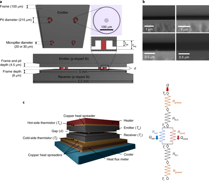
Standalone devices are manufactured by separating the surfaces by pillars. The structural integrity of the device depends on the number of pillars and their diameter; the larger is the contact area between the pillars and the surfaces, the better it is from a robustness standpoint. The pillars however introduce a pathway for heat to flow by conduction, and the conduction rate between the surfaces increases linearly with the contact area. Similarly, sub-500-nm pillars lead to large conduction rate, as conduction is inversely proportional to the pillar length. To minimize conduction while ensuring the device structural integrity, we manufactured pillars with large diameters (20 μm to 30 μm) that are much longer than the gap spacing into micrometre-deep pits etched into one of the surfaces. The device structural integrity enables visualizing the gap spacing via scanning electron microscopy (SEM), as shown in the figure below. We cannot understate the importance of SEM imaging in our work. By visualizing the gap spacing, we were able to directly assess the quality of the device (presence and uniformity of gap spacing). All devices that passed the SEM quality control step resulted in successful heat transfer measurements.

Now that we have robust near-field radiative heat transfer devices, the next step is to think about engineering applications. We hope that our work will spark the implementation of energy conversion and thermal management technologies capitalizing on near-field radiative heat transfer.
Follow the Topic
-
Nature Nanotechnology
An interdisciplinary journal that publishes papers of the highest quality and significance in all areas of nanoscience and nanotechnology.


Please sign in or register for FREE
If you are a registered user on Research Communities by Springer Nature, please sign in