Discovery of Single-defect Memristor
Published in Electrical & Electronic Engineering

When I was a 1st year Ph.D. student in Prof. Deji Akinwande’s group in 2015, our group had reported state-of-the-art flexible transistors and pioneered wearable applications based on two-dimensional (2D) material. The question then came to me whether I can contribute something new in order to realize a complete flexible system, for example, other essential components such as memory devices. In the same year, Prof. Hersam’s group reported planar 2D memory based on monolayer MoS2. However, the observation is only favorable with a special kind of grain boundary, and as such it is difficult to control it.
Thus, the vertical metal-insulator-metal (MIM) structure stood out, which is the preferred structure for emerging memory in the industry with the added benefit of 3D integration capability. However, it is the conventional thinking in metal oxides that resistance switching cannot scale down below a few nanometers because of excessive leakage. I did not give up since 2D materials can usually have very different properties from the bulk, especially considering their crystalline nature in contrast to disordered metal oxides. My supervisor, Prof. Akinwande, is very open-minded and always encourages and supports us to try out new ideas. In the context of a high failure probability, Xiaohan Wu, who is my main collaborator, and I were surprised to observe stable non-volatile resistive switching (NVRS) in monolayer MoS2 and we first reported this discovery in the desired MIM configuration in 2018 (Nano Lett. 2018, 18, 1, 434–441). We further discovered the thinnest memory device based on monolayer h-BN in 2019 (Adv. Mater. 2019, 31, 1806790). We called these atomically-thin memory devices atomristors.
One of the most outstanding applications for resistive switching behavior is for information storage. In addition, we charted a brand-new application, radio-frequency (RF) switches used in wireless and communication systems (radio, 5G and terahertz frequencies) with state-of-the-art figure of merit based on MoS2 and h-BN atomic sheets (Nature Communications volume 9, Article number: 2524, 2018, and Nature Electronics, volume 3, pages 479–485, 2020).
After the systematic study of NVRS behavior, optimization, and application at the device level, the fundamental mechanism behind the resistive switching was still a mystery. Solving this mystery required more fundamental and atomic level investigations. At the end of 2017, Prof. Akinwande and I wrote a user proposal to Oak Ridge National Lab to start atomic-level studies on this topic. Initial images of MoS2 layers obtained with the scanning tunneling microscope (STM) were promising. However, observing the sequence of events leading to NVRS required far more than getting images of the atomistic layers. A few months later, Dr. Saban Hus, who was a postdoctoral researcher at Oak Ridge National Lab and an expert in transport measurements with STM and Multi-probe STM systems, joined our team. He frequently traveled back to Oak Ridge to conduct the STM experiments and focused on the defects as a potential source of NVRS.
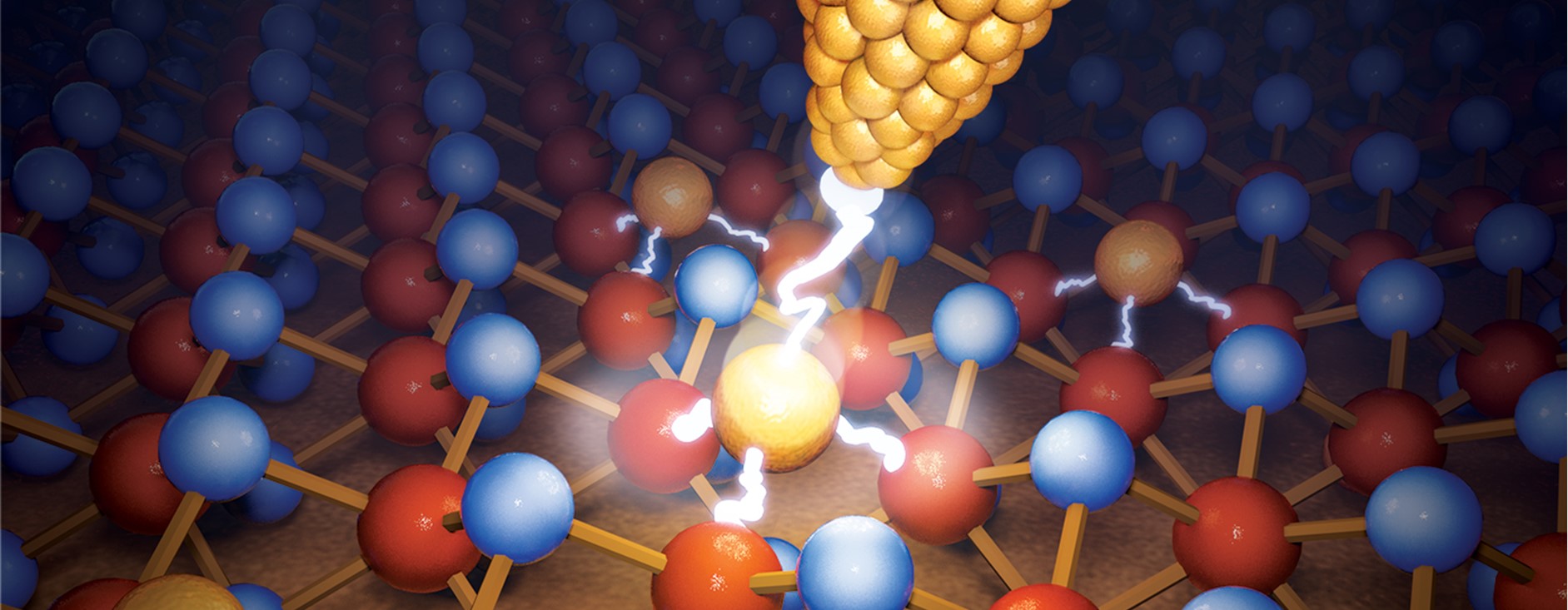
Switching an atomic layer's resistance requires a physical modification of its atomic arrangements, either from a pristine structure to a defective one or between two defective structures. STM was the perfect (possibly the only) tool to observe and create such modifications in a controlled fashion. Saban used gold STM probes to mimic MIM structures at the nanometer scale and observe the modifications on the MoS2 atomic sheet before and after resistive switching events. Given the fragile nature of atomically sharp STM probe and limited control on individual atoms' movement, it took many months of experiments to get conclusive results. At the end, we showed that the resistive switching occurs when a sulfur vacancy is filled with a metal atom migrating from the electrode.

Once these experiments concluded, we did not only solve the mystery behind the resistive switching in 2D monolayers, but we also created the smallest memristor unit, which switches its resistance by the controlled movement of a single gold atom between the electrode and a sulfur vacancy in the MoS2 layer. This was the first direct observation of the switching behavior at the atomistic level in monolayer crystalline films. But the work has a broader implication on the functionalization of defects in 2D materials. With a better understanding of physical mechanisms of resistive switching behavior and new capabilities to alter the defects with atomic precision, we hope to inspire further scientific and applied research in the utilization of atomic defects for applications from high-density memory to quantum computing.
For more information please check out our article “Observation of single-defect memristor in an MoS2 atomic sheet” published in Nature Nanotechnology.
Follow the Topic
-
Nature Nanotechnology
An interdisciplinary journal that publishes papers of the highest quality and significance in all areas of nanoscience and nanotechnology.


Please sign in or register for FREE
If you are a registered user on Research Communities by Springer Nature, please sign in
well done! congrats
Wonderful work, congratulations !