Enhanced photovoltaic effect in graphene–silicon Schottky junction under mechanical manipulation
Published in Electrical & Electronic Engineering

In this article, we introduced an electromechanical method based on the flexoelectric effect to enhance the photovoltaic (PV) efficiency in graphene-silicon Schottky junctions (GSJs). By applying a strain gradient through atomic force microscope (AFM) tip-based indentation, the open-circuit voltage (Voc) of GSJs is observed to increase by up to 20%, leading to a significant improvement in power conversion efficiency. The findings suggest that strain gradient holds potential for the development of GSJ-based flexo-photovoltaic applications, opening new opportunities for large-scale manufacturing and integration in Schottky solar cells.
Due to its special two-dimensional structural properties and excellent performance, graphene has the potential to be integrated into existing semiconductor technologies and used in next-generation electronics. Recent research has shown that the formation of junctions between graphene and three-dimensional (3D) or two-dimensional (2D) semiconductors can produce the rectification effect of a typical Schottky junction. Its tunable Schottky barrier makes graphene junctions an excellent platform for studying the transport properties of interfaces and has led to applications in scenarios, such as photodetection, light-speed communication, and chemical and biological detection. Solar energy collection and conversion have attracted much attention in recent years. The Schottky junction devices can naturally work as solar cells, photovoltaic cells, or as the built-in electrical field providing the voltage potential difference that drives the current. Conventional metal/semiconductor Schottky devices suffer from the contact instability, high cost, and high temperature fabrication process. Graphene, which has unique optical properties and excellent mechanical properties, offers Schottky solar cell with low sheet resistance, high optical transparency, large area growth, and low-cost transferring. Over the last decade, many studies have been focused on a Gr/Si Schottky junction (GSJ) for solar cell applications. An overall power conversion efficiency (PCE) of 1%–1.7 % is achieved with an open circuit voltage (Voc) and a short circuit current (JSC) linearly depending on the intensity of incident light. By chemical doping, PCE can be further increased for 8:5%. With systematical optimization, including the number of graphene layers, PCE can surpass 3%. Furthermore, substrate metasurface, such as Si nanowire, Si nanohole array, and additional antireflection layer, are proposed for PCE enhancement.
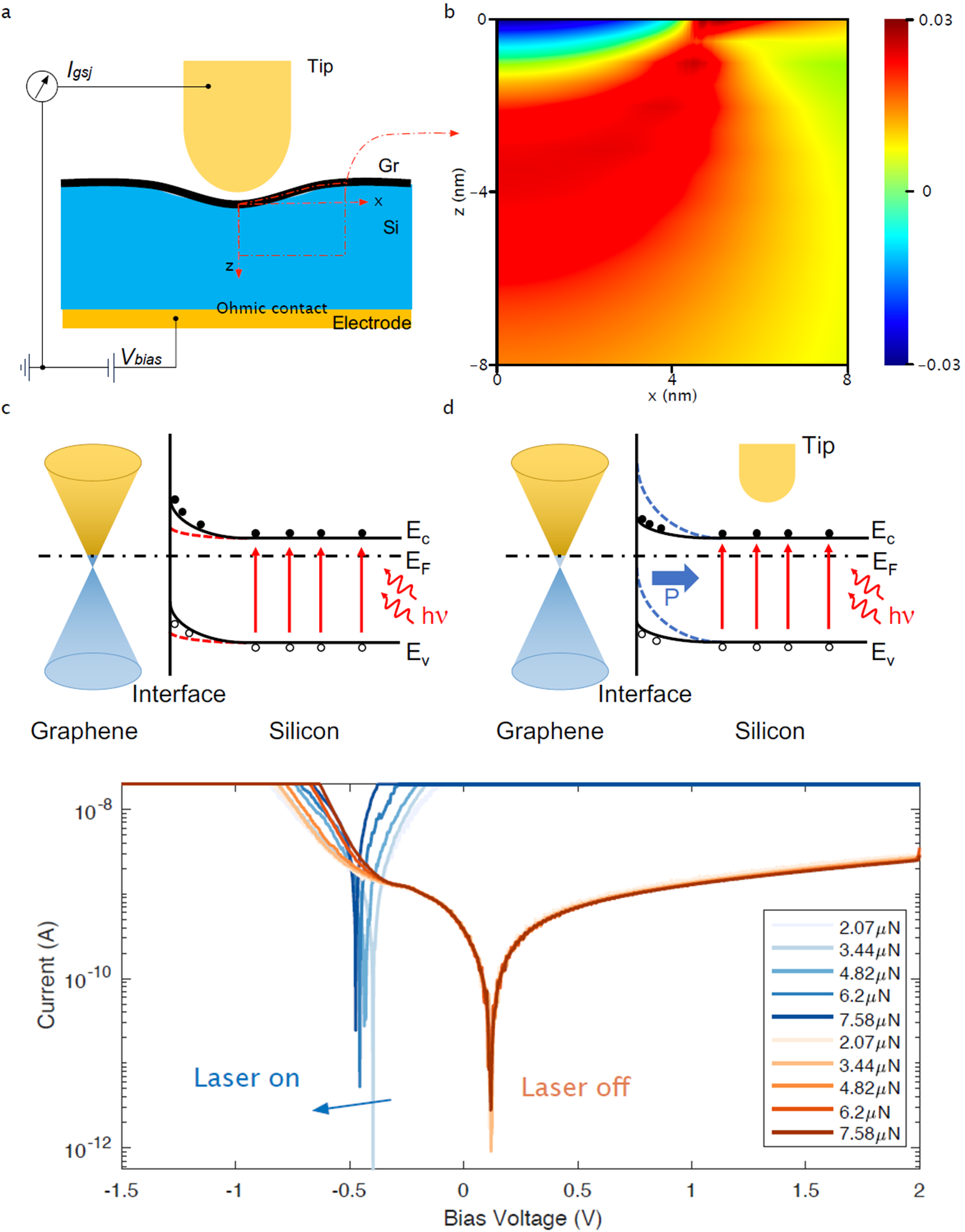
However, one primary limitation for the GSJ Schottky solar cell is the low open circuit voltage Voc, which relates to the small Schottky barrier height (SBH). Here, we introduce an electromechanical coupling, called flexoelectricity, to increase the SBH, thus, to enhance the performance of GSJ solar cell. The flexoelectric effect describes the linear coupling between electric polarization and strain gradient in solid state materials. It suggests that the polarization can originate from the strain gradient even in the centrosymmetric systems. Compared with the piezoelectric effect that has extensively been studied, the response of the flexoelectric effect is very weak and remains underexplored. The electric polarization induced by the strain gradient is typically of the order of 10-9 at the macro scale. As the geometric size scales down, the strain gradient is inversely proportional to the spatial scale. Thus, the micro-nano-structure is used to achieve a large strain gradient, and the flexoelectric effect is induced by the strain gradient and dominates over piezoelectric effect at nanoscale. In recent years, by using atomic force microscope (AFM) to introduce the large strain gradient, a number of experimental studies concentrating on the mechanism of flexoelectricity and its applications have emerged.
In this study, we introduce the flexo-photovoltaic effect in the Gr/Si Schottky junction. We find the GSJ performance as a solar cell can be largely enhanced through the flexoelectric effect by using AFM tip pressing. By in situ adding mechanical force on the GSJ, the current flowing through the junction to the tip can be detected, then being read out based on a CAFM module using AFM. The current–voltage curves under different applied forces are analyzed, and we obtained the corresponding SBH variation as a function of the applied force. Under illumination, the GSJ device shows the PV effect. Voc can be improved by this electromechanical effect. We finally demonstrate the enhanced PV through the flexoelectric effect in GSJ. The graphene/silicon junction Schottky devices are prepared with a single layer of CVD graphene being wet-transferred to the lightlydoped n-type silicon layer forming the two-dimensional and threedimensional (2D and 3D) Schottky contacts. The bottom of the silicon substrate is mechanically scraped to remove the thin oxide layer and coated with GaIn and copper to form an ohmic contact.33 The scanning electron micrograph (SEM) of the device is shown in Fig. 1(a). The graphene covers the silicon window (dark area) forming the Schottky contact, connects with the Au electrode (surrounding gray part), and forms ohmic contact with Au electrodes. The graphene is etched to ribbons. The surface morphology of the Gr ribbon edge tested by AFM is shown in Fig. 1(b).Theleft-handsideflatten area is silicon covered by graphene, while the other is bare silicon after graphene being etched. With the tip contacting the GSJ area, the current can be read out with the CAFM module. Figure 1(c) shows the high spatial resolution current distribution of the junction with Vbias=-1V. Figure 1(d) shows the corresponding Raman mapping on the graphene ribbon device.
The short-circuit current (Jsc) cannot be directly obtained, because of the instrument current-limits. Nevertheless, the photoresponse [in Figs. 3(a) and 3(b)] implies that this GSJ device has an evident photovoltaic effect. To further investigate the mechanical manipulation of the PV effect, we applied forces by AFM nano-indentation on the GSJ. We first turn the laser off to study the force induced effects on the GSJ. The response current (absolute value) in the forward bias area can be enlarged by increasing the applied force [Fig. 3(c)]from 2:07 to 7:58 uN, while the response current in reverse bias area maintains being cut off. Similarly, for each applied force, we then collect the current data by sweeping the bias voltage Vbias when turning the laser on, shown in Fig. 3(d). In the forward bias area, the GSJ current (IGSJ ) maintained being enlarged (absolute value) when the applied force is increased in contrast to Fig. 3(c). Due to the laser induced photoresponse, the current dramatically changed. There exists an evident photovoltaic area. By directly contrasting the I–V responses under different applied forces, the half-logarithmic graph of the absolute GSJ current as a function of bias voltage is shown in Fig. 4(a). For the laser-off cases (orange lines), the open-circuit voltage Voc remains stable under different applied forces. Remarkably, for the laser-on cases (blue lines), due to the existing photovoltaic effects, Voc varies from near zero to -0:5 V in contrast to the laser-off cases. The absolute value of Voc is increased from 0:38 to 0:46 V for more than 20%, as shown in Fig. 4(b) (the blue circles). Fitting the laser-off cases with Eq. (1), the Schottky barrier height as a function of applied forces is obtained, as shown in Fig. 4(c). The strain gradient in the substrate originates from the contacts between the tip and the substrate surface, which breaks the inverse symmetry in the silicon20,28 and cause an extra flexoelectricity induced built-in potential in addition to the native depletion layer in the GSJ. The SBH can be additionally increased by the forces.

Please sign in or register for FREE
If you are a registered user on Research Communities by Springer Nature, please sign in