Graphene Channel Electron-Multiplying Charge-Coupled Pixel
Published in Electrical & Electronic Engineering

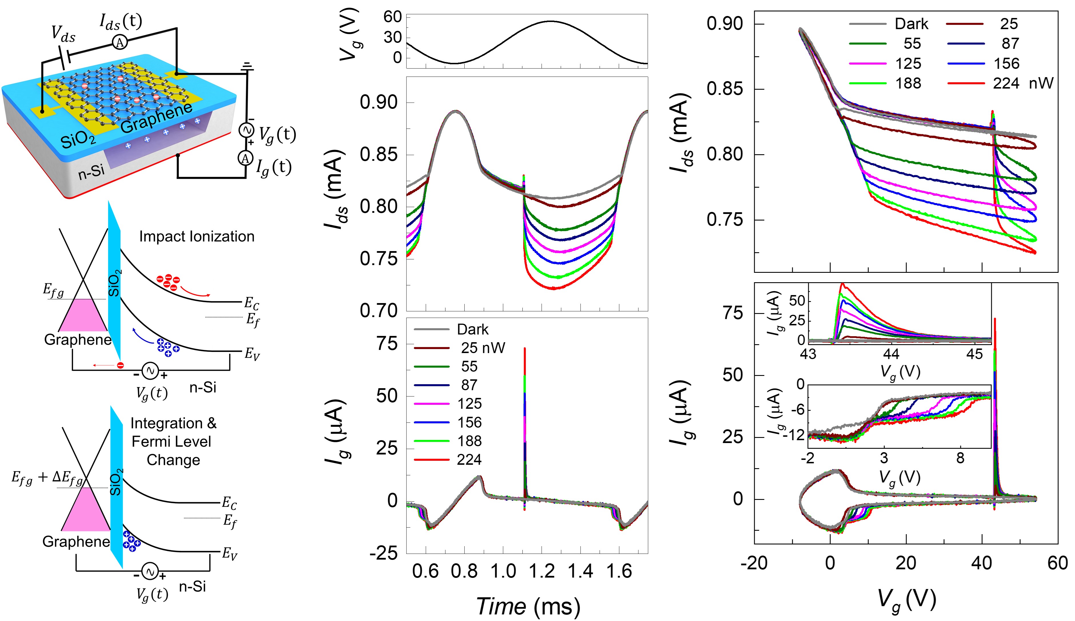
In this work, for the novel GCCD pixel, CM, which dictates the intrinsic gain in optoelectronic devices, is in-pixel realized in the out-of-plane geometry by exploiting strong silicon surface potential instead of relying on traditional gate-to-gate coupling used in traditional EMCCDs. By offering an in-situ readout of CM due to its capacitive coupling with the silicon photogate, the graphene channel mimics the random access mode used in the CMOS imager. A fast sinusoidal gating signal drives the pixel into pre-avalanche condition, followed by pulsed illumination. Once photo carriers undergo multiplication, the self-regulation mechanism tunes the silicon surface potential and, successively, the MF. The maximum MF and responsivity of 8.5 and 350 A/W are attained, respectively. The proposed sinusoidal drive is more suitable for applications like surveillance, adaptive optics, and LiDAR, where power dissipation control is more critical than the linearity of operation.
Electron-multiplying charge-coupled device (EMCCD) technology has been implemented in low-light surveillance, photon-starved scientific instrumentation used in astronomy, low-light microscopy, and photon counters. In comparison, modern CCD concepts are finding exciting applications, such as ultra-sensitive calorimeters, dark matter detection, and exoplanet imaging quests. Multiple square-like H/L phase clocks are applied to the conventional CCD pixels to serially transfer The associate editor coordinating the review of this manuscript and approving it for publication was Huamin Li . the photo charges to the readout circuit, as the readout circuit and integration processes are independent. The conventional surface channel CCDs suffer from charge transfer inefficiency (CTI) arising from multiple factors like edge effect, varying transfer times, variable trap occupation, and capture during transfer, particularly for large transfer electrodes phased at a frequency less than 1 MHz. For a CCD applied for detecting a weak and faint burst of photons, the interface traps and CTI are considered major limiting factors that are coped with by implementing a FAT ZERO charge in the device at all times.
The traditional problem of clock-induced charge (CIC) originating from the large H/L switching of the square phase clocks can be dealt with by implementing a traveling (sinusoidal) clocking/driving setup for CCDs [11]. Moreover, the sinusoidally driven CCD can reduce the power consumption to the minimum limit, eliminate the field-free zones in the interpixel regions, and subside the interface defects. The sinusoidal drive is more suitable for applications like surveillance, adaptive optics, and light detection and ranging (LiDAR), where control of power dissipation is more critical than linearity of operation.
Carrier multiplication (CM) in CCDs is a post-detection process. It can be realized during carrier transport under a strong electric field (∼ 3 × 10⁷ V/m) between adjacent depletion wells separated by the potential barrier with an approximate thickness of 1 μm. Therefore, carriers are often subjected to backscattering, recombination, and surface defects, leading to increased CTI.
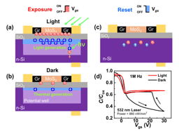
Direct photoconduction graphene detectors exhibit responsivities less than 100 mA/W owing to the carrier transport distances in photodetectors are often much higher (∼100 μm) than the recombination lengths of ∼ 1 μm in graphene with ∼ 2 ps of carrier recombination time. Hence, the collection of the photo-induced electron-hole (e−h) pairs within the graphene channel becomes challenging. To overcome this issue, conventional device schemes such as metal-oxide-semiconductor(MOS) field-effect transistors, image sensors, and protection elements can be realized in which graphene can be introduced to enrich the functionality of the devices. By capitalizing on the silicon photo-gating through fieldeffect coupling, a transparent, charge-sensing graphene layer can detect photo-generation within a thicker adjacent substrate rather than serving as the fundamental lightabsorbing medium. The changes in the graphene channel conductance can be sensed by the application of bias voltage allowing channel current (Ids). This current is directly proportional to the carrier density(n) and mobility(μ) of graphene (Ids ∝ μnE). Graphene’s high ambipolar mobility (∼ 103 − 105 cm2 /V.s) offers a significant built-in gain that can further enhance the detector’s response. For such graphene-based photogated devices, responsivities higher than 1, 000 A/W have been reported. The holes in the silicon quantum well, imaging the same number of electrons in the graphene readout channel, increasing the conductivity of initially n-doped graphene is already reported. This tunability of graphene in the MOS structure can combine the benefits of existing imaging technologies, permitting more flexible handling of the charge packets. Such graphene-based CCD schemes for direct readout in a broad wavelength range have been recently reported.
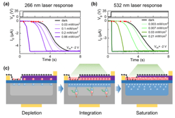
This work studies the effect of photoexcitation in the pre-avalanche condition of the GCCD pixel. The prospect of detecting the out-of-plane impact ionization in silicon photogate via Ids as an alternative to displacement current(I g), is also testified. The GCCD pixel is set into the dynamic preavalanche state by applying fast sinusoidal gate voltage(Vg) to the semiconductor substrate. When the device was exposed to a pulsed illumination, the initial photogenerated carriers experience the pre-avalanche condition, increasing the displacement current (I g) to a peak value. The initially multiplied photo carriers integrate at the semiconductor-oxide interface(Si/SiO2) and start screening the electric field, causing a decrease in the relative change in Ig, and multiplication factor (MF) which is defined as the ratio of the photocurrent peaks in the avalanche and depletion regimes. Due to this shielding effect, the avalanche current returns back to the equilibrium state, and a steady-state Ig is re-established. This distinctive selfregulating phenomenon occurring in the MOS structure can be enhanced in the GCCD pixel due to the strong field-effect of graphene.
The initial charge packet resulting from the detection of weak photon burst experiences pre-integration CM, which boosts the signal-to-noise (S/N ) ratio, hence removing the need for FAT ZERO charges. This non-destructive, uninterruptible, and in-situ photo-hole detection significantly improves the responsivity and readout speed. Finally, insights regarding the transient photoresponse of the GCCD pixel are also presented, which opens a new avenue for 2D3D hybrid photo sensors. The rest of this paper is organized as follows. Section II provides details of GCCD pixel fabrication and related measurement schemes. Section III(A) comprises basic device characterization, followed by (B)an explanation of the self-regulation mechanism which not only tunes CM but also helps to understand the (C) transient photoresponse of the device. Transfer characteristics of sinusoidally–driven GCCD pixel under pulsed illuminations are presented in (D). In(E), a comprehensive discussion on overall reduced power consumption under such biasing is presented along with (F)calculations of performance parameters. In Section IV, we concluded our work.
When the CCDs fabricated on the high resistivity semiconductor substrate, usually used in back-illuminated scenarios, are not sufficiently thinned, the electric field does not evenly extend throughout all the substrate thickness, and field-free regions cause dark diffusion current. In our case, the GCCD pixel is not fabricated on the high-resistivity substrate nor back-illuminated. Still, diffusion from the fieldfree region(bulk silicon and surrounding area of the GCCD pixel) can occur. The silicon space charge region thickness for sinusoidal biasing varies continuously compared to an almost fixed thickness space charge region for square biasing, while the measurements are performed at room temperature. Thus, we have neglected the field-free diffusion phenomenon in our calculations.
IEEE Access ( Volume: 11) Page(s): 37424 - 37436

Please sign in or register for FREE
If you are a registered user on Research Communities by Springer Nature, please sign in