Graphene Field-Effect-Coupled Detection of Avalanche Multiplication in Silicon
Published in Electrical & Electronic Engineering
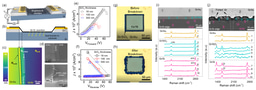
In this work, we demonstrate the instant detection of out-of-plane avalanche multiplication in graphene-oxide-semiconductor structure via strong field-effect coupling of the graphene channel with the silicon photo gate. This in-situ detection of out-of-plane avalanche can eliminate carriers’ pre-amplification losses in traditional avalanche multiplication charge-coupled devices. By relying upon the electrostatic coupling, a real-time signature of the space charge region in silicon can be observed by both displacement and channel currents of the device. This allows us to alternatively probe the multiplication capability of the graphene-oxide-semiconductor structure under pulsed laser illumination while the semiconductor is dynamically biased through multiple ramping signals. The operating scheme of the device shows good capability for detecting weak light (45 nW), while the intrinsic self-regulating mechanism helps avoid oxide breakdown. The maximum multiplication factor of the responsivity of 340 , and specific detectivity of 2.85 × 10¹³ Jones are achieved, respectively.
CHARGE-COUPLED device (CCD) offers applications in astronomy, low light microscopy, and photon counters due to their high sensitivity and wide linear dynamic range. Multiple phase clocks are applied to the conventional CCD pixels for serial transfer of the photo charges to the readout circuit as the charge readout, and charge integration processes are independent. Carrier multiplication (CM) in CCDs is a postdetection process. It can be realized during carrier transport under a strong electric field (∼ 105 V/cm) between adjacent depletion wells separated by the potential barrier with an approximate thickness of 1 μm. Therefore, carriers are often subjected to backscattering, recombination, and surface defects.
Direct photoconduction graphene detectors exhibit responsivities less than 100 mA/W. It is because the carrier transport distances in photodetectors are often much higher (∼100 μm) than the recombination lengths of ∼1 μm in graphene with ∼2 ps of carrier recombination time. Hence, the collection of the photo-induced electron–hole (e–h) pairs within the graphene channel becomes challenging. Alternatively, instead of using graphene as a photo absorber, it can be adapted in conventional device schemes such as metal-oxide-semiconductor (MOS) field-effect transistors, flexible image sensors, and protection elements to enhance the functionality of the device.
By benefitting from the electrostatic capacitive coupling, a tunable monolayer graphene sheet can sense the photo-ionization in adjacent photogating semiconductor substrate instead of an active light-absorbing medium. The changes in the graphene channel conductance caused by the capacitive coupling can be probed through channel current (Ids) by applying the fixed biasing voltage where Ids is directly related to carrier density (n) and mobility (μ) of graphene. 1Ids will replicate the photocurrent in the space charge region of silicon photogate. Moreover, its high transparency (97.7%) allows almost all of the illuminated light to penetrate into the photogate, hence eliminating the need for thinner metallic electrodes and anti-reflection coatings in conventional devices, i.e., MOS. In contrast, its high ambipolar mobility can be a source of large built-in gain and resultantly enhance the detector’s response. For such photo-gated graphene devices, responsivities up to 2500 A/W have already been reported.
The holes integrated into the well image the same number of electrons in the graphene readout channel, leading to an increase in the conductivity of graphene. This nondestructive, uninterruptible, and in situ charge readout of the potential well significantly improves responsivity and speed. The self-sensing ability of graphene in the MOS structure can bridge the advantages of CCD and CMOS technologies allowing flexible manipulation of the information signal (charge packet). Such graphene-based CCD schemes for direct readout in a broad wavelength range from X-ray to mid-infrared (MIR) have already been implemented.
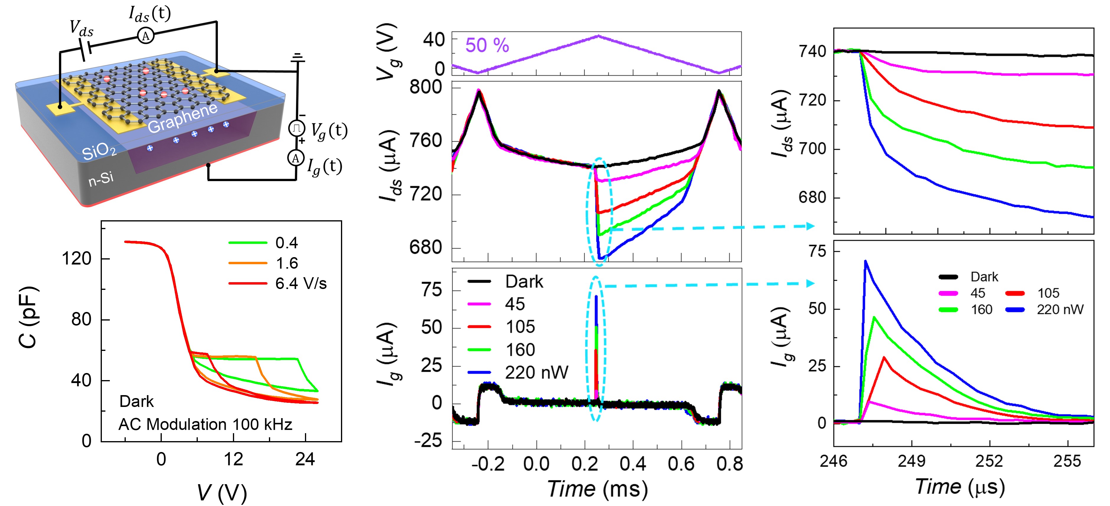
The dynamic I –V characterization of the MOS device showing the competition between the fast-sweeping gate voltage (Vg) and the surface potential (φSi) has been reported. The effect of photoexcitation in the preavalanche condition of the graphene-oxide-semiconductor structure, working as graphene charge-coupled device (GCCD) pixel is investigated in this study. The GCCD pixel is driven into the preavalanche condition by applying the fast ramp Vg to the semiconductor substrate. When exposed to a pulsed laser, the initially photoexcited carriers that experience the preavalanche condition raise the displacement current (I g) to a peak value. The very first multiplied photocarriers integrate at the oxide-semiconductor interface and shield the electric field, leading to a decrease in the relative change in Ig and the multiplication factor (MF) due to screening. In response to this shielding effect, the avalanche current comes back to the equilibrium, and a steady-state Ig establishes across the interface.
The unique self-regulating phenomenon occurring in the MOS structure can be enhanced in the GCCD pixel due to the strong field effect of graphene. Along with the plausibility of detecting the impact ionization phenomenon via Ids, alternatively to Ig, the predictions about the ramp rate dependence of the multiplication phenomenon are tested. Moreover, the insights regarding the transient photoresponse of the GCCD pixel are also presented. This technique opens a new avenue for 2D-3D hybrid photo sensors.
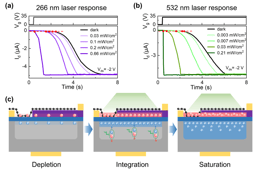
The notion of in situ photodetection (sensing through Ids) for sweeping gate bias and fastly switching ON/OFF square wave bias is shown in Fig. 3. The creation of a potential well by quasi-statically reverse biasing the silicon substrate, followed by a 532-nm constant laser illumination and subsequent sensing of integrated charges through Ids is depicted in Fig. 3(a). Multiple laser intensities are implemented while Vds= 10 mV. Moreover, by offering several output current levels, the GCCD pixel can be used as multilevel logic technology. A fast square Vg signal having switching duration of only 5 ns promptly drives the GCCD pixel into deep depletion state. An almost constant dark condition Ids in reversed biased scenario emphasizes the small thermal charge generation and successive integration at the Si/SiO2 interface. Then, the capability of the GCCD pixel for multibit photo memory application is demonstrated by monitoring the minority carrier integration via Ids (stair-like response) for multiple 915-nm pulsed illuminations, as shown in Fig. 3(b). Only the reverse biased condition is plotted as in the accumulation state, no obvious photoresponse is experiential.
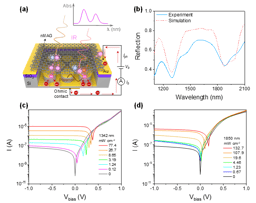
For pulsed light illumination onto the GCCD pixel, the photo generation vertical to the Si/SiO2 interface exhibits a decaying exponential signature with the maximum at the Si/SiO2 interface and 1/e of the maximum at ∼40 μm away from the interface into the substrate, as the penetration depth of a 915-nm laser is 200 μm. For our GCCD structure, 15.84% of Pt reflects while the remaining 84.16% transmits into the substrate [47] and collectively produces e–h pairs inside the space charge (∼ few μm thick) and bulk (which is larger than the potential well thickness xd by two orders) regions. Approximately 93% of photons are not photo-ionizing in the active well region as they are either reflected or absorbed inside the bulk region.
When the GCCD pixel is ramped into avalanche condition, Ig and Ids flowing in the GCCD structure in response to the pulsed optical excitation will sense the internal gain. The magnitude of this gain depends on the initial MF and the rise time of the photon flux. The ramp rate controls initial value of MF (when the pulsed light is turned on in the avalanche regime, the very first photo-generated carriers will undergo avalanche multiplication similar to the thermally generated carriers in the dark, which can be high up to 106), and the instantaneous value of MF during the light pulse is further affected by screening due to the increasing inversion-layer charge.
IEEE Transactions on Electron Devices ( Volume: 70, Issue: 5, May 2023), Page(s): 2370 - 2377
Prof. Yang Xu is an IEEE NTC Distinguished Lecturer, Fellow of the Institute of Physics (FInstP), Fellow of Institute of Engineering and Technology (FIET), Fellow of Royal Society of Chemistry (FRSC), Fellow of the Institute of Materials, Minerals and Mining (FIMMM), and IEEE Senior Member of the Electron Devices Society. He received his B.S. degree in Institute of Microelectronics at Department of ECE from Tsinghua University, M.S. and Ph.D. degrees in ECE from the University of Illinois Urbana-Champaign (UIUC), USA. He is now a full professor at the School of Micro-Nano Electronics, Zhejiang University, China. He was also a visiting by-Fellow of Churchill College at the University of Cambridge, UK, and a visiting professor at the University of California Los Angles (UCLA). He has published more than 120 papers including Nature Nanotechnology, Nature Electronics, Nature Photonics, Chemical Reviews, Advanced Materials, Chemical Society Reviews, Nature Communications, Nano Letters, ACS Nano, and IEDM,etc. He holds over 30 granted patents and gave more than 50 talks in international conferences. He is also served as Associate Editor of IEEE T-ED, Photonics Research, and IEEE Nanotechnology Magazine, Editorial board member of IOP Nanotechnology, Microelectronics Journal, Micro & Nano Letters, and IET Circuits, Devices & Systems, Advisory Panel Member of IOP Nanotechnology, and was TPC committee members of IEEE-EDTM, IEEE-IPFA, and IEEE-EDAPS conferences. His research interests include emerging 2D/3D integrated optoelectronic devices for Internet-of-Things and Post-Moore Ubiquitous Electronics.


Please sign in or register for FREE
If you are a registered user on Research Communities by Springer Nature, please sign in