High-Performance Broadband Graphene/Silicon/Graphene Photodetectors: from X-ray to Near-Infrared
Published in Electrical & Electronic Engineering

In this article, we report a high-performance broadband graphene/thin silicon/graphene (GSG) photodetector by realizing a synergistic combination of graphene and silicon absorption bandwidths from the X-ray to near-infrared (NIR) regions. The sensitivity of the proposed photodetector in this spectral range is greatly enhanced. A high responsivity of 0.56 A/W, a high detectivity of 2.72 ×10¹¹ Jones, and a fast response time of 7.2 ns are achieved. Moreover, the real-time array imaging at broadband regions presented in this study can benefit from the independent pixel structures similar to the complementary-metal-oxide-semiconductor (CMOS) architecture. This approach constitutes a reliable route toward a high-performance photodetector with a prominent broad-spectrum response, high responsivity, and low noise. These results will motivate strategies to achieve high-performance, broadband image sensors, compatible for on-chip CMOS circuit technology that advances the development of next-generation graphene/silicon image sensors.
As a fundamental building block of optoelectronic integrated circuits, photodetectors are increasingly becoming an essential component in image sensing, biochemical detection, and optical communication due to their high detection efficiency and fast response speed. Broad spectrum detection is crucial in many application areas such as earth remote sensing, environmental monitoring, and autonomous vehicles. However, realizing a high-performance photodetector with ultrabroad spectrum photoresponse, especially covering the x-ray–ultraviolet (UV)–visible–near-infrared (NIR) range, is still a major challenge. In most cases, traditional semiconductors with wideband gaps (WBGs), such as silicon carbide (SiC), zinc oxide (ZnO), and gallium nitride (GaN) are generally employed in UV photodetectors as they are transparent to visible light and contain strong chemical bonds. Nevertheless, the properties of WBG semiconductor-based detectors are limited by the quality of the oxide layer and surface states/defects, leading to slow photocurrent recovery that hinders their usage in high-speed detection applications. In addition, there are challenges in terms of enhancing the sensitivity, response speed, integration level, and signal-to-noise ratio in ultrabroadband detection. Graphene shows great potential in broadband detection due to its unique absorption properties. Therefore, graphene as an active layer in Metal–semiconductor–metal (MSM)based photodetectors can significantly improve photon absorption, response speed, photoelectric conversion efficiency, and sensitivity. We fabricate a graphene/thin silicon/graphene (GSG) structure to meet the growing requirements that include high resolution, miniaturization, and low power consumption of the silicon-based broadband optoelectronic integrated system.
Here, we demonstrate high-performance detection using a GSG photodetector, which outweighs its drawbacks with the benefits from the combined absorption spectra of graphene and silicon. The broadband absorption of the GSG structure and high energy radiation detection of Si capacity allow the device to exhibit high responsivity (0.56 A/W at 375 nm), fast response speed (7.2 ns), high quantum efficiency (85.2%), and broadband detection range from x-ray to NIR. The 8 × 8 arrays of the GSG photodetectors further demonstrate the device integrability in a large matrix of sensors. In addition, as our device structure is compatible with other graphene-like 2D materials, it presents a device scheme with excellent complementary-metal-oxide-semiconductor (CMOS) compatibility. The GSG photodetector opens an avenue to explore ultrabroad spectral response while paving the way for superior-performing graphene/silicon-based optoelectronic devices for real-time applications.
The devices were fabricated by a standard silicon-on-insulator (SOI) wafer with a 1 lmthick,1–10 X cm resistivity top n-type silicon. ASiO2 layer with 100-nm thick was grown using plasma-enhanced chemical vapor deposition (PECVD) as an insulating layer on the top Si. Then, the Ti/Au (15 nm/60 nm) contacts were formed through lithography and e-beam evaporation and treated by a liftoff process. A Si window was patterned by lithography and buffered oxide etchant (BOE). High-quality CVD-grown single-layer graphene (SLG) was transferred onto the Si window.15 The SLG interdigitated (IDT) structures were patterned by lithography and etched by the O2 plasma. Finally, a wire bonding was performed to connect the device with the designed printed circuit board (PCB). The electrical measurements were performed by a Tektronix Source Measure Unit 2450 and a semiconductor analyzer (FS480, PDA Co. Ltd.). The lasers provided UV light with wavelengths of 266 and 375 nm. The x-ray detection was accomplished by a commercial Amptek-mini-X2 x-ray tube with a maximum power of 10 W. The xray photon energy and the dose rate can be tuned correspondingly by adjusting the voltage and the current of the x-ray tube, respectively. Visible and NIR light were applied by the 532, 915, and 1064 nm lasers for broadband tests. The power of the laser source was measured by an optical power meter (Thorlabs S120VC) with the applicable sensor. The time-dependent response was accomplished by connecting the device and the trans-impedance amplifier (TIA) (DHPCA-100, FEMTO, 200 MHz bandwidth) with an oscilloscope (Agilent DSO 9404A, 4 GHz bandwidth). The absorbance measurements were conducted at room temperature using a HITACHI U-4100 UV–vis–NIR spectrometer.
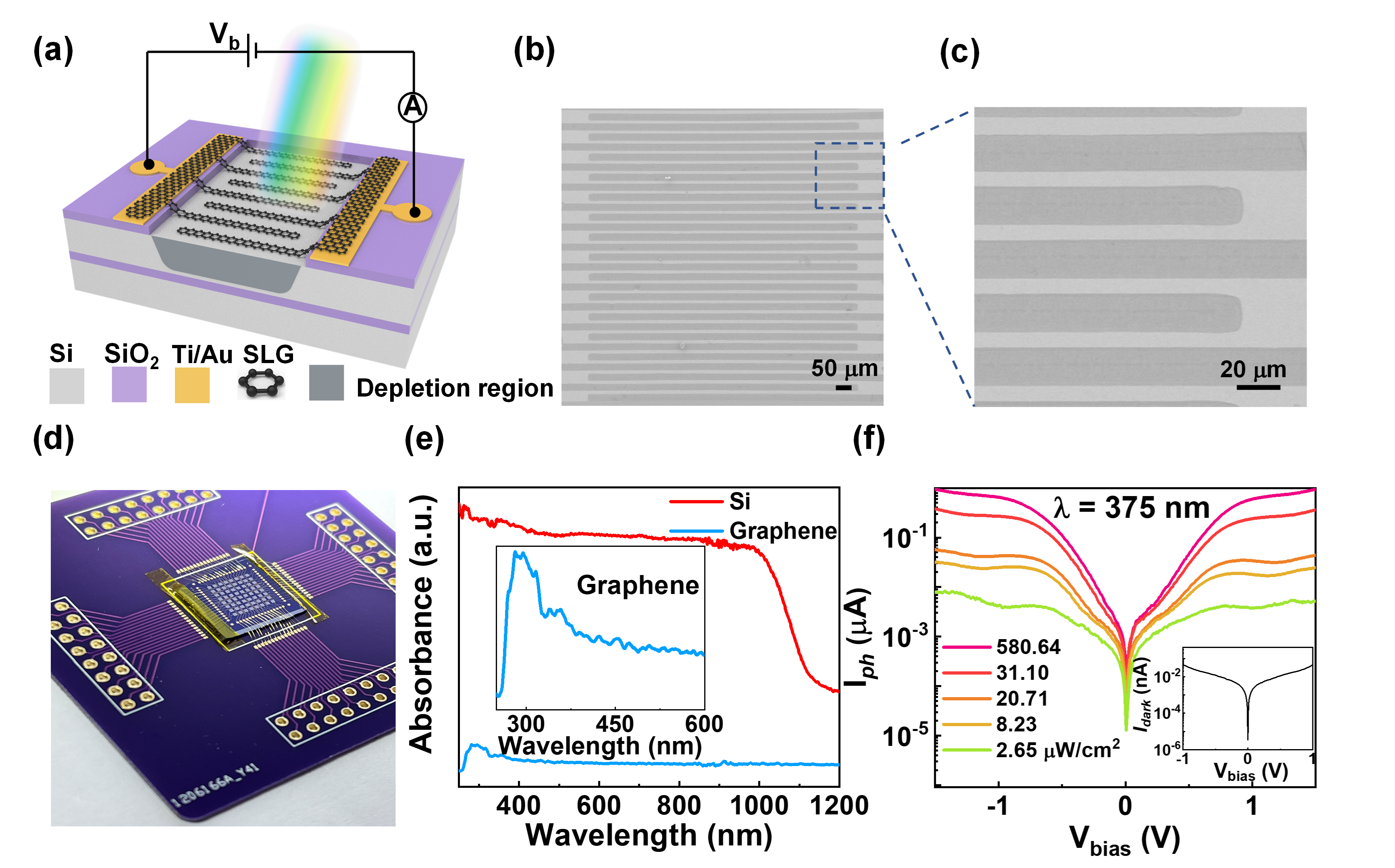
The schematic structure of the GSG photodetector with the simplified equivalent circuit is shown in Fig. 1(a). The photograph of the 8 8 bonded photodetector arrays [Fig. 1(d)] indicates the potential of our devices in the CMOS integration technique. Figure 1(b) displays the scanning electron microscopy (SEM) image and (c) the zoomed-in image of the single-layer graphene (SLG) interdigitated (IDT) structure consisting of 30 graphene fingers, which shows the uniformity of the graphene. The Raman spectra of graphene show characteristic G and 2D bands around 1585 and 2678 cm 1,respectively.The large 2D to G peak intensity ratio (I2D/IG > 1) confirms the monolayer nature of the CVD-grown graphene, and the strong G peak and the weak D peak indicate good graphitic quality, which demonstrates the graphene owns high crystallinity with carrier mobility.
We investigate the SLG IDT structure to form our GSG photodetector. Graphene shows a remarkably extended lifetime of photoinduced hot carriers, especially in the UV wavelength range, and it is noted that the device sensing capability increases with an increase in the gap between the interdigitated fingers. Using the Landauer formula, the Schottky barrier height (SBH) of 0.51 eV can be extracted by considering the diffusion of photo carriers and the thermionic emission model. Photonic enhancement is from thermionic emission through the low-interface recombination Schottky junction. The light absorption from both SLG and Si contributes to the high density of photo-charged carriers, which helps maintain high sensitivity over the broadband range. When the wavelength of incident light 1.1 um, such as UV light, some of the light is absorbed by graphene at the M point of the Brillouin zone. As UV has short penetration depth in Si, the majority of the photo-generated carriers exist near the Si surface under illumination. Simultaneously, most of the photons are absorbed by the Si substrate and excite electron–hole pairs in Si, which separate directly in the Si depletion region to form photocurrents. The junction helps in separating the electron–hole pairs without massive combination, which results in high responsivity. The IDT SLG structures have high-resolution characteristics, which is conducive to construct highperformance, nondestructive imaging systems.
Applied Physics Letters, Volume 12215, February 2023, Pages 071105

Please sign in or register for FREE
If you are a registered user on Research Communities by Springer Nature, please sign in