High-performance near-infrared OLEDs maximized at 925 nm and 1022 nm through interfacial energy transfer
Near-infrared (NIR) light (>700 nm) is widely used in biomedical diagnostics such as infrared photodynamic therapy, wearable oximeters (high tissue penetration depth), distance sensing in the automotive industry, and defense applications. As far as light sources are concerned, the current mainstream commercial products are semiconductor near-infrared light-emitting diodes (LEDs). However, the lack of both flexibility and miniature properties limits their extensibility to modern applications. As for alternatives, on the one hand, focus is on the quantum dots (QDs) and perovskites NIR LEDs. They, however, encounter difficulty in long-term stability and environmental issue. On the other hand, researchers also explore the organic materials incorporated LEDs in NIR, dubbed as NIR-OLEDs. Unfortunately, organic near-infrared emission is often limited by the emission gap law, stating that the heat dissipation rate increases exponentially as the emission gap decreases due to the increase of exciton-vibration coupling. Therefore, most organic NIR emitters are weakly emissive, making challenging the high performance NIR-OLEDs. To circumvent this obstacle, from 2017-2023, we have successfully applied self-assembly of Pt-complexes to reduce the exciton-vibration coupling, and made breakthrough in attaining high performance Pt-complexes associated NIR-OLEDs. Despite this great success, the underlying concern is that the required specific Pt-complexes greatly limit the diversity of organic molecules. We thus began to mull how to engineer the NIR-OLEDs using the known Pt-complexes as a platform, which then couple with the NIR organic dyes to enhance the NIR emission and thus NIR-OLEDs. In this article, we provided a solution using a method of interfacial energy transfer. As a result, we double the radiative brightness by well organizing the packing and accordingly improve the external quantum efficiency (EQE) by a factor of ten for the NIR-OLEDs using commercially available NIR dyes. Three criteria are require to account for the success of “interfacial energy transfer” process:
- The photoluminescence of the energy donor (Pt(II) complexes) must overlap with the absorption spectrum of the energy acceptor. The former requires a strong photoluminescence quantum yield (PLQY), and the latter necessitates a high absorption coefficient.
- For an energy donor and an energy acceptor to function effectively, there must be a sufficient difference between their energy levels. If the LUMO levels overlap, this would lead to charge distribution evenly rather than localized at the interface, resulting in an adverse effect. HOMO levels would exhibit analogous phenomena.
- OLEDs must be optimized to bring electron-hole recombination near the interfacial zone within the effective Förster Resonance Energy Transfer (FRET) distance, so that energy can be transmitted effectively.
Dilemma and Turning point
Initially, we chose a reported phosphorescent material with a high photoluminescence quantum yield (PLQY ~80%), Pt(fprpz)₂, as the energy donor (fulfilling the first criterion). Subsequently, we selected an NIR absorber widely used in organic photovoltaics (OPV), BTP-eC9, as the energy acceptor (simultaneously fulfilling the first and second criteria). However, our initial thought faced great challenge. Pt(fprpz)₂ could not dissolve in any solvent and could only form thin films through evaporation deposition, while BTP-eC9 could only be spin-coated. We then thought about simply spin-coating BTP-eC9 onto Pt(fprpz)₂ to achieve interfacial energy transfer. Unfortunately, things did not go as planned. Directly spin-coating BTP-eC9 onto Pt(fprpz)₂ resulted in strong physical interpenetration, which led to the failure of interfacial energy transfer. To reduce the interpenetration, we then proposed a stamping method, a technique widely applied in transferring two-dimensional materials. Through surface contact, thin films can be transferred. Eventually, we successfully achieved interfacial energy transfer using the stamp method and produced high-efficiency NIR-OLEDs. We also experimented with two other sets of materials, proving that our solution was not a coincidence. The stamp method will be a general and viable approach for the process of interfacial energy transfer.
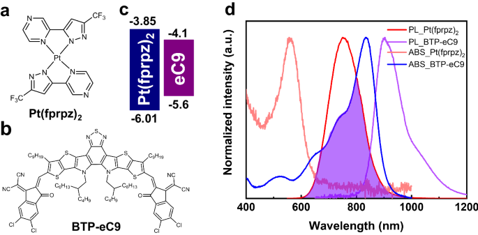
General information on Pt(fprpz)2 and BTP-eC9. a Chemical structure of Pt(fprpz)2 and b BTP-eC9 molecules, along with c their energy levels. d Absorption and emission spectra of Pt(fprpz)2 and BTP-eC9, with the overlapping region indicating the radiative energy transfer zone.
Mechanism and morphology
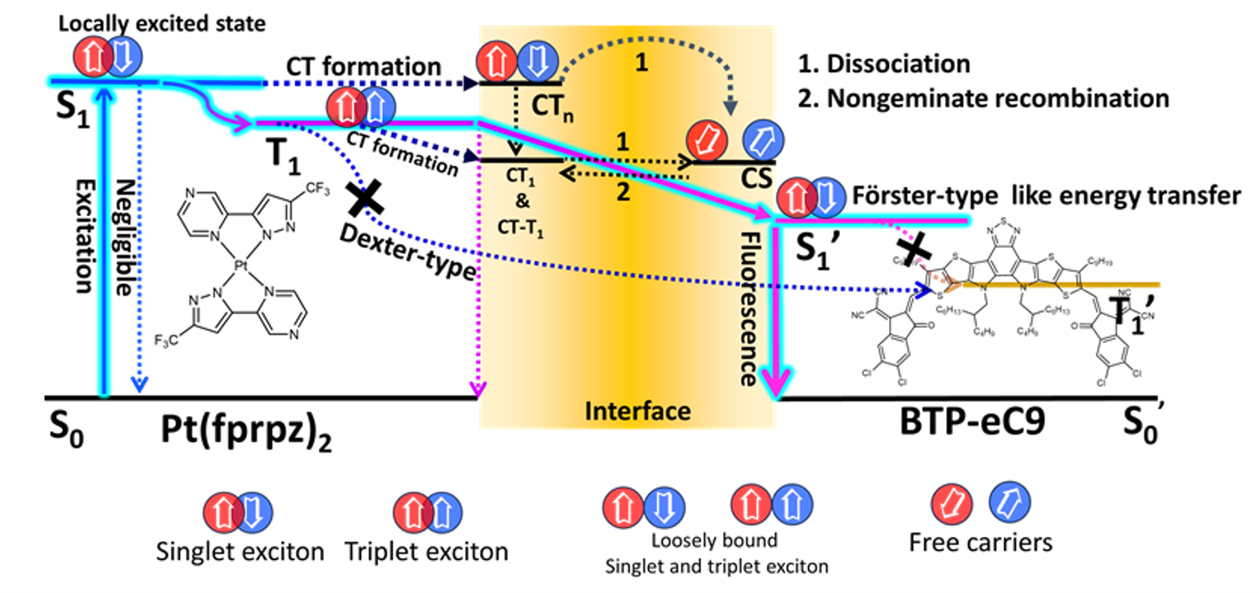
When the material is operated as a device, electronic excitation always results in a 25% singlet (S) and 75% triplet (T) population according to spin statistics. At room temperature, typical organic emitters does not emit light in the triplet state due to its spin forbidden transition. If we cannot harvest the populated triplet state back to the emitting singlet state, efficiency of electroluminescence will be greatly limited. In this study, we proposed to use phosphorescent Pt(II) materials as donors to perform energy transfer from the triplet state to other emitting organic material. Due to the strong spin-orbit coupling caused by the heavy Pt atom, ultrafast intersystem crossing from S1 to T1 occurs in Pt(fprpz)2, resulting in a 100% T1 population. Förster-type energy transfer, which transfers energy from the T1 of Pt(fprpz)2 to the S1 of BTP-eC9, allowing BTP-eC9, which otherwise can only harvest 25% from the populated S1 state, to achieve 100% S1 state, resulting in high efficiency.
The result of photon luminescence-mapping and atomic force microscopy (AFM) clearly indicates the difference between stamp method and spin coating. The morphology of Pt(fprpz)2 remained unchanged using the stamp method but was destroyed causing shorten emission lifetime and poor efficient with spin coating. Grazing-incidence wide-angle X-ray scattering (GIWAXS) not only supported the observation above but found the shorten d-spacing of the parallel planes of BTP-eC9 in the stamped film, enhancing the radiative transition, hence the PLQY.
For further characterization, as one of the Y-family derivatives, there are lots of report about picosecond-transient absorption spectra (ps-TAS) of BTP-eC9. The 780nm signal, which was previously assigned to charge separation (CS), is undesirable in OLED because CS is one of non-radiative decay channels. Compared to the spin coating, stamp method shows much weaker CS signal, implying the smoother interface and less non-radiative deactivation.
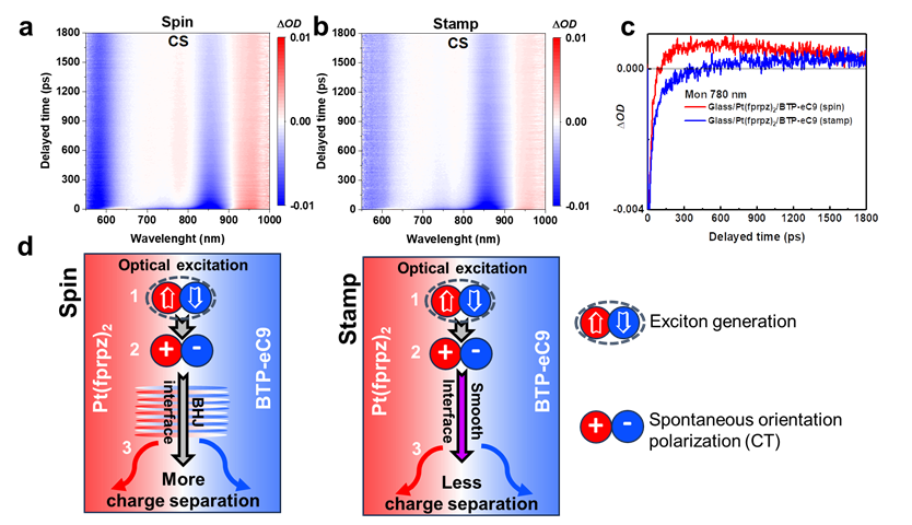
TA results of films treated with spin or stamp methods. Pseudo-color plots of the picosecond transient absorption (ps-TA) spectra for a Pt(fprpz)2/BTP-eC9 spin-coated film and b Pt(fprpz)2/BTP-eC9 stamped film. c The time-dependent transient absorbance (ΔOD) of Pt(fprpz)2/BTP-eC9 spin-coated and stamped films was monitored at 780 nm. d Schematic diagram of exciton dynamics at interfaces prepared by different methods. Process (1): Optically excited exciton generation. Process (2): The spontaneous orientation polarization in the interface facilitates the charge-transfer (CT) formation and (3) subsequent charge separation (CS). Left of d: The bulk heterojunction (BHJ) formed due to spin-coating leads to abundant interfaces, providing sufficient driving force for CT formation that undergoes charge separation. Right of d: The smooth and plane interface produced by stamping facilitates the production of fewer CT states and, thus, fewer CS separations.
Optimization and fabrication
It is important to recognize that Y11 is one of the best NIR-OLED emitters currently available. So, why don’t we use Y11, but instead opt for BTP-eC9? Here is our explanation: Although Y11 and BTP-eC9 share similar structural and optical properties, Y11 exhibits a 1.5-fold increase in radiance and external quantum efficiency (EQE) when incorporated into a device. Interestingly, Y11 does not perform optimally when used in current transfer processes. This is because the LUMO level of Y11 nearly aligns with that of Pt(fprpz)2. Therefore, charges are split evenly to the two materials rather than localized at the interface, limiting the efficiency of interfacial energy transfer. Subsequent simulations with Setfos software clearly demonstrated that a larger difference in the LUMO levels between the materials increases the probability of luminescence at the interface, and the same applies to HOMO levels.
Ultimately, we selected Pt(fprpz)2 as the energy donor and BTP-eC9 as the energy acceptor. However, we observed that using a 10nm layer of Pt(fprpz)2 resulted in poorer transfer effects compared to a 5nm layer due to the overall thickness exceeding the Förster resonance energy transfer (FRET) distance, causing most charge recombination occurring within Pt(fprpz)2. Further simulations with Setfos software revealed that a sandwich structure of Pt(fprpz)2/BTP-eC9/Pt(fprpz)2 achieves higher efficiency. Consequently, the final NIR-OLED device exhibited an emission wavelength of 925nm, an EQE of 2.24%, and a radiance of 39.97 W sr-1 cm-2, which is a tenfold improvement in EQE and a twofold increase in brightness compared to a device using only BTP-eC9. To demonstrate the broad applicability of this method, we extended the emission wavelength to 1022nm, achieving similar enhancements with an eightfold increase in EQE to 0.66% and a twofold increase in radiance to 18.67 W sr-1 cm-2.
For further information, please check our latest article in Nature Communications (https://doi.org/10.1038/s41467-024-49127-x).
Follow the Topic
-
Nature Communications
An open access, multidisciplinary journal dedicated to publishing high-quality research in all areas of the biological, health, physical, chemical and Earth sciences.

Related Collections
With Collections, you can get published faster and increase your visibility.
Women's Health
Publishing Model: Hybrid
Deadline: Ongoing
Tumor Microenvironment Crosstalk and Therapeutic Implications
Publishing Model: Hybrid
Deadline: Nov 02, 2026


Please sign in or register for FREE
If you are a registered user on Research Communities by Springer Nature, please sign in