
Oxidation of copper is something we often encounter, not only when working as scientists and engineers but even more frequently in daily life. In many cases we will consider its results a nuisance, for instance tarnished surfaces or degradation of electrical device performance. However, oxidized copper can be more than a corrosion product as the most common oxidation states, i.e. Cu2O and CuO, show favorable physico-chemical characteristics that can be harnessed in photovoltaics, catalysis and environmental sensing applications. Here, we will focus on Cu2O and its unique optical properties at cryogenic temperatures. This material has been extensively studied over the last decades, in particular for achieving excitonic Bose-Einstein condensation and due to the fascinating characteristics of Rydberg excitons with high quantum numbers. Surprisingly, most experiments relied on geological bulk samples, which motivated us to explore excitons in synthetic micrometer-sized Cu2O crystals.
In our recent article, we demonstrate the growth of high-quality Cu2O microcrystals via a scalable thermal oxidation process. Figure 1 shows scanning electron microscope images of the sample morphology (top-view and cross-sectional image in left top and left bottom panel, respectively). Photoluminescence spectroscopy down to milli-Kelvin temperatures showed very low defect and impurity levels. Moreover, photoluminescence from Rydberg excitons was observed (Figure 1, right panel) in a wide range of excitation conditions. The energy levels of the Rydberg excitons followed a quantum number dependence similar to a hydrogen atom.
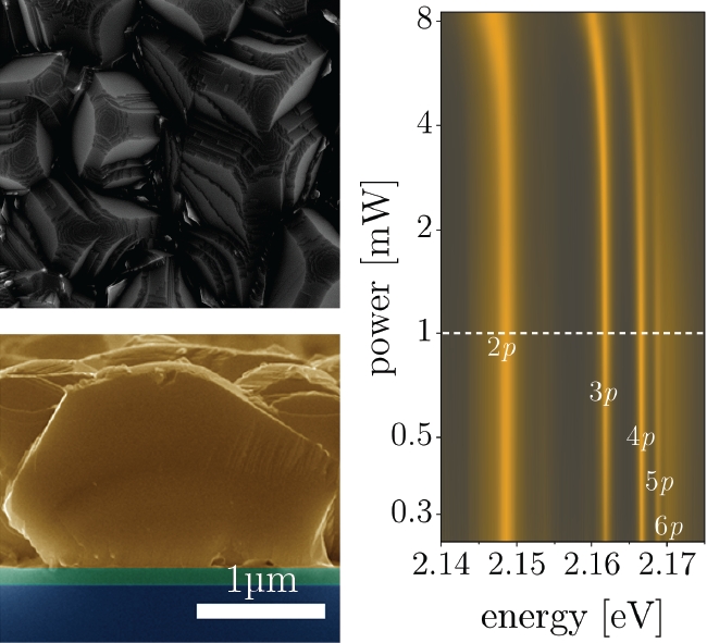
showing photoluminescence from Rydberg excitons of the yellow n-p series.
One major advantage of our growth method is its compatibility with standard silicon fabrication techniques and the possibility for photonic circuit integration. In particular, site-controlled Cu2O microcrystal growth can be combined with silicon nitride waveguide technology (Figure 2). We demonstrate on-chip waveguide coupling of free exciton emission at room temperature, paving the way for future device technologies based on this material.
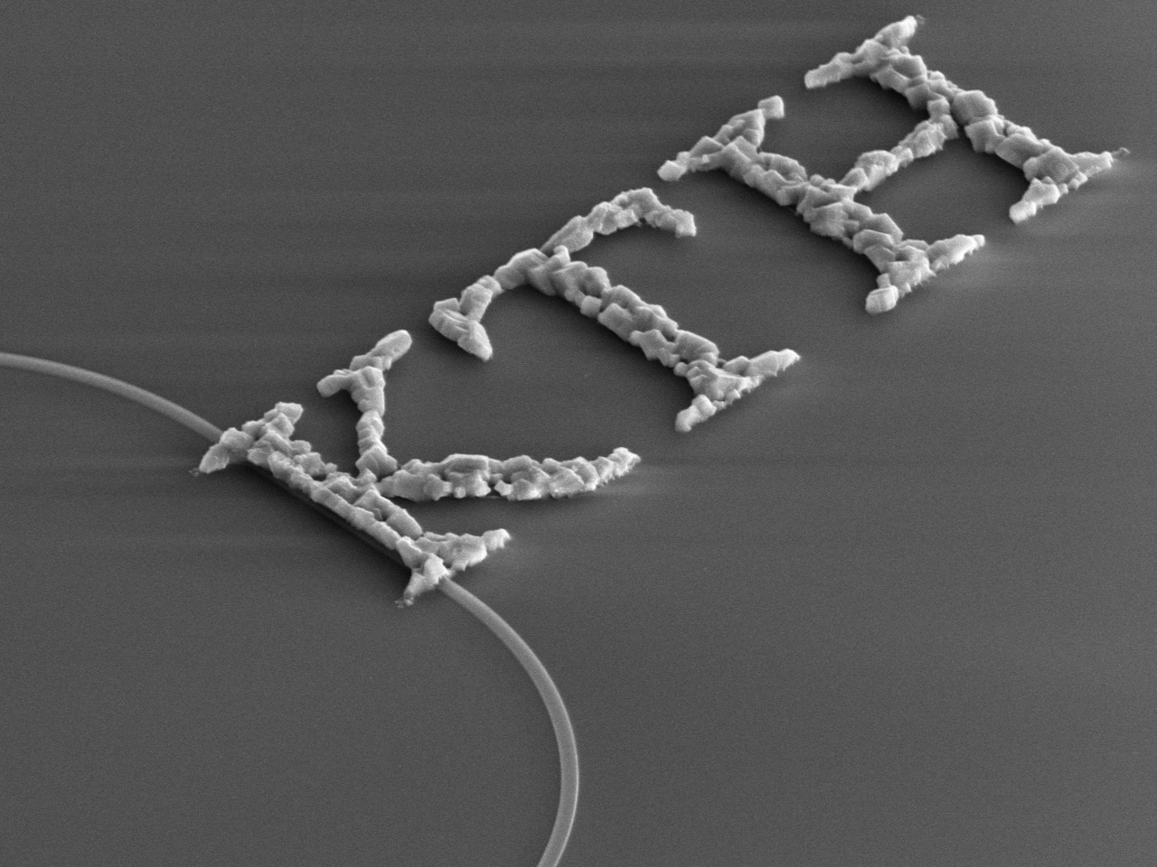
on-chip coupling to silicon nitride-based photonic waveguides.
Cu2O takes a special position as the three-dimensional semiconductor capable of hosting giant Rydberg excitons with high principal quantum numbers. Such Rydberg excitons have attracted significant interest in the scientific community as they show properties analogous to atomic Rydberg states, which are considered a highly promising system for applications in quantum information processing. Our work lays the foundation for realizing quantum technologies based on solid-state Rydberg excitations that can be interfaced with photonic integrated circuits, aiming at on-chip generation and manipulation of light at the single-photon level. Hence, exciting challenges lie ahead to translate quantum information processing and quantum sensing schemes previously developed for Rydberg atoms into the solid-state environment of a semiconductor crystal at the micrometer or nanometer scale.
For more information, please see our recent publication in Communications Materials:
Stephan Steinhauer, Marijn A. M. Versteegh, Samuel Gyger, Ali W. Elshaari, Birgit Kunert, André Mysyrowicz, Val Zwiller. Rydberg excitons in Cu2O microcrystals grown on a silicon platform. Communications Materials 1, 11 (2020).
https://doi.org/10.1038/s43246-020-0013-6
Follow the Topic
-
Communications Materials
A selective open access journal from Nature Portfolio publishing high-quality research, reviews and commentary in all areas of materials science.
Related Collections
With Collections, you can get published faster and increase your visibility.
Materials for quantum sensing and computing
Publishing Model: Open Access
Deadline: Jul 09, 2026
Triboelectric nanogenerators for energy harvesting
Publishing Model: Open Access
Deadline: Jun 30, 2026
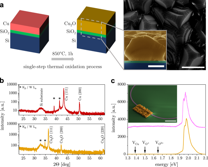






Please sign in or register for FREE
If you are a registered user on Research Communities by Springer Nature, please sign in