In-Situ Monitoring of Reciprocal Charge Transfer and Losses in Graphene-Silicon CCD Pixels
Published in Electrical & Electronic Engineering
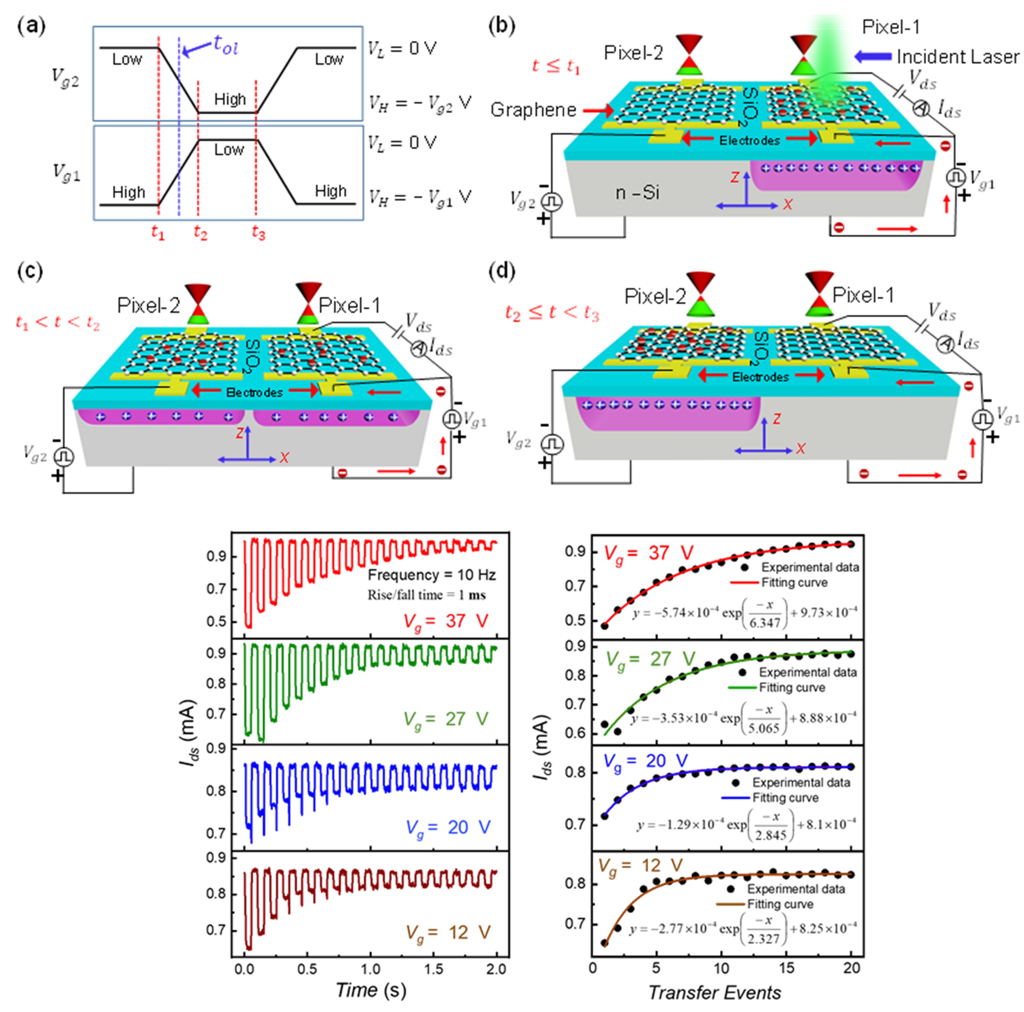
Charge-coupled devices (CCD) allow imaging by photodetection, charge integration, and serial transfer of the stored charge packets from multiple pixels to the readout node. The functionality of CCD can be extended to the non-destructive and in-situ readout of the integrated charges by replacing metallic electrodes with graphene in the metal-oxide-semiconductors (MOS) structure of a CCD pixel. The electrostatic capacitive coupling of graphene with the substrate allows the Fermi level tuning that reflects the integrated charge density in the depletion well. This work demonstrates the in-situ monitoring of the serial charge transfer and interpixel transfer losses in a reciprocating manner between two adjacent Gr-Si CCD pixels by benefitting the electrostatic and gate-to-gate couplings. We achieved the maximum charge transfer efficiency (CTE) of , which is mainly decided by the inter-pixel distance, phase clock amplitudes, switching slopes, and density of surface defects. The discussion on overcoming transfer losses and improving CTE by realizing a graphene-electron multiplication CCD is also presented. The proof of the concept of the in-situ readout of the out-of-plane avalanche in a single Gr-Si CCD pixel is also demonstrated, which can amplify the photo packet in a pre-transfer manner.

Photoexcited carrier integration and multiplication play a pivotal role in developing efficient photodetection, especially for weak incident light. Charge-Coupled Devices (CCD) and Complementary Metal-Oxide-Semiconductor (CMOS) are two leading imaging technologies with specific advantages and disadvantages. The attractive factors for using the CCD are its simple metal-oxide-silicon (MOS) photogate detector, which offers high sensitivity, high fill factor, and low noise. For CMOS imagers, the independent pixel structure provides random access, simple clocking, fast parallel readout, natural antiblooming, and low power consumption. Emerging imaging technologies require benefits from both CCD and CMOS architectures. Whereas all major imaging technologies based on CCD and CMOS often suffer from loss of image quality and contrast due to extensive transport and weak charge-to-voltage conversion efficiency. Graphene can provide absorption tunability that can extend to UV to terahertz band by electrically adjusting the Fermi level without any additional manufacturing cost. Unique properties of graphene open opportunities in various application areas, such as photodetectors, chemical sensors, and metamaterial absorbers that even extend to environmental cleanup functionalities and protection units. Graphene-based photodetectors often exhibit responsivity within 100 mA/W, resulting from short carrier recombination time (~2 ps) and recombination length (~1 μm), while the charge transport lengths in photodetectors are often extending to hundreds of microns. Thus, collecting photo-induced carriers before recombination within the graphene channel is still a challenging task. One of the approaches to overcome this issue is integrating graphene with conventional device architectures like CCD and CMOS.
Graphene can work as an atomically-thin, transparent, charge-sensing layer that, by leveraging upon the photogating phenomenon through electrostatic capacitive coupling, detects absorption within a thicker adjacent substrate rather than serving as the lightabsorbing medium. The changes in the graphene channel conductance can be sensed by the application of a constant bias voltage causing channel current (Ids). This current is proportional to the product of carrier density (n) and mobility (μ) of graphene (Ids ∝ μnE). Moreover, graphene’s significant ambipolar mobility provides a built-in photo gain mechanism that can enhance the detector response. For photo-gated graphene devices, responsivity higher than 1000 A/W has been reported. This photo gating of graphene offers a solution to the previously mentioned issue by allowing a hybrid imaging scheme that adopts the benefits of both CCD and CMOS architectures while providing a direct readout of the integrated photoexcited charge and allowing flexible manipulation of the information signal (charge packet).
Previous works have demonstrated the potential of graphene-based CCD schemes for direct readout in a broad wavelength range from X-ray to mid-infrared (MIR). The next crucial step towards large-scale Gr-Si CCD imagers is to realize direct readout of charge multiplication and integration within the charge domain via graphene. A large number of serial transfers in CCD structure at high electric fields sufficient to trigger impact ionization leads to charge amplification within the charge domain before the charge-tovoltage conversion. In this work, we present the proof of concept for in-situ monitoring of the serial charge transfer between adjacent Gr-Si CCD pixels and investigate the potential of this platform to achieve charge multiplication in reciprocating neighboring pixels. Moreover, the proof of the concept of the in-situ readout of an out-of-the-plane avalanche in silicon absorber through displacement (Ig) and graphene channel (Ids) currents are explored as well in this work. The Gr-Si CCD pixel is initially dynamically ramped into deep depletion. At this stage, pulsed laser excitation triggers an avalanche effect via photoionization in the device that can be sensed by the two probe techniques discussed above.
Parasitic capacitance often causes unwanted oscillations at the output of the circuit during the extended frequency operation of electronic devices. Whereas the operational frequencies of Vg1 and Vg2 reported in this work (10 Hz) are too low to cause any feedback loop. Another possible contribution of parasitic capacitance might originate from the proximity effect based on interpixel distance. However, the dimensions of our individual Gr-Si CCD pixels and corresponding interpixel distance (5 μm) are long enough to supress any such proximity effects to cause parasitic capacitance. Therefore, parasitic capacitance is not a dominating factor in our reciprocating charge transfer process.
In Figure 5a, CTE is plotted vs. phase amplitude (Vg) for switching durations of (10, 100, 500, and 1000) μs. The increasing fringing field and slow switching rates result in higher CTE’s. For almost all the gate bias values and switching slopes of two phases, a decaying trend in the first ∆Ef g of the readout graphene is observed. It shows the attenuation of the initial photo charge packet instead of any multiplication. We demonstrate that by exploiting random access and serial transfer modes together, the properties of CCD and CMOS technologies can be overlapped, allowing more flexible operation.
The proposed device scheme uses three pixels as a single unit enabled by the serial charge transfer. The photo charges in these three adjacent MOS capacitors are temporarily held in the detector by a barrier until the avalanche unit is ramped to a strong fringing field. So, three clock phases are applied to three adjacent Gr-Si CCD pixels platforms (∼1 μm distance). This platform can boost CTE and transfer speed benefitting from the random access and serial transfer modes. In Figure 5b, the 3D schematic and related circuitry are shown. The direct readout is implemented for the avalanche unit connected with Vg3, while Vg1 and Vg2 are associated with the detector and transfer units.
The displacement current is not an appropriate readout probe for traditional CCDs having multiple rows and columns requiring multiple top-gating phases to transfer carriers from one pixel to the next until they reach the readout sense node. Contrary to that, the displacement current can be used for direct readout of an out-of-plane avalanche event (zdirected) from a single Gr-Si CCD pixel. Moreover, this out-of-plane carrier multiplication due to the electrostatic coupling of the Si/SiO2 interface with the top tunable graphene channel can be in-situ readout through Ids. The measurement scheme for recording the Ig and Ids currents while silicon is dynamically biased is shown in Figure 6a. This measurement scheme is the same as the single-pixel characterization scheme shown in Figure 1a. The only difference is the application of a fast ramping biasing signal.
Sensors 2022, 22(23), 9341; https://doi.org/10.3390/s22239341
Prof. Yang Xu is an IEEE NTC Distinguished Lecturer, Fellow of the Institute of Physics (FInstP), Fellow of Institute of Engineering and Technology (FIET), Fellow of Royal Society of Chemistry (FRSC), Fellow of the Institute of Materials, Minerals and Mining (FIMMM), and IEEE Senior Member of the Electron Devices Society. He received his B.S. degree in Institute of Microelectronics at Department of ECE from Tsinghua University, M.S. and Ph.D. degrees in ECE from the University of Illinois Urbana-Champaign (UIUC), USA. He is now a full professor at the School of Micro-Nano Electronics, Zhejiang University, China. He was also a visiting by-Fellow of Churchill College at the University of Cambridge, UK, and a visiting professor at the University of California Los Angles (UCLA). He has published more than 120 papers including Nature Nanotechnology, Nature Electronics, Nature Photonics, Chemical Reviews, Advanced Materials, Chemical Society Reviews, Nature Communications, Nano Letters, ACS Nano, and IEDM,etc. He holds over 30 granted patents and gave more than 50 talks in international conferences. He is also served as Associate Editor of IEEE T-ED, Photonics Research, and IEEE Nanotechnology Magazine, Editorial board member of IOP Nanotechnology, Microelectronics Journal, Micro & Nano Letters, and IET Circuits, Devices & Systems, Advisory Panel Member of IOP Nanotechnology, and was TPC committee members of IEEE-EDTM, IEEE-IPFA, and IEEE-EDAPS conferences. His research interests include emerging 2D/3D integrated optoelectronic devices for Internet-of-Things and Post-Moore Ubiquitous Electronics.


Please sign in or register for FREE
If you are a registered user on Research Communities by Springer Nature, please sign in