Nature-inspired micropatterns
Published in Bioengineering & Biotechnology, Earth & Environment, and Materials
Micropatterned materials have developed in nature over 3.8 billion years, with remarkable performance. Nature inspiration is the process of understanding biological mechanisms and strategies and using this knowledge to solve technical problems or enhance engineering designs. The term nature inspiration includes biomimetics, biomimicry and bioinspiration. Micropatterns are patterned materials or structures that have feature sizes in the nanometre-to-micrometre range. Owing to size effects, micropatterns can impart novel functions to a material without altering the bulk composition and properties. By imitating natural strategies, engineering challenges can be solved. Examples include mimicking ecological and in vivo microenvironments or producing superhydrophobic surfaces, adhesives and structural colours. Nature inspiration is an interdisciplinary field, involving various materials and fabrication techniques. This Primer provides a comprehensive overview of nature-inspired micropatterns, which offer unique design strategies and functional properties. In this Primer, key principles, fabrication methods and applications of nature-inspired micropatterns are discussed. Additionally, future prospects and challenges are highlighted for this rapidly evolving field.
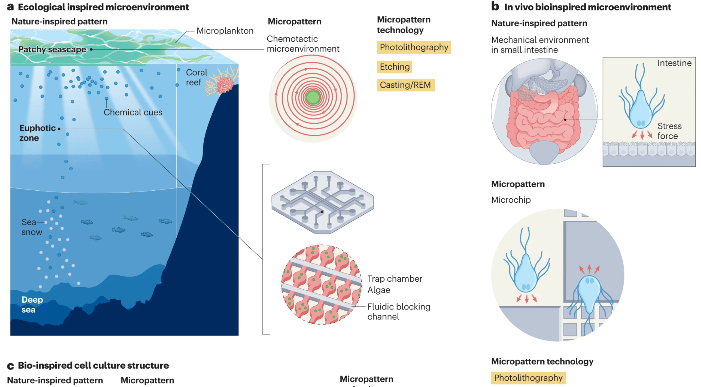
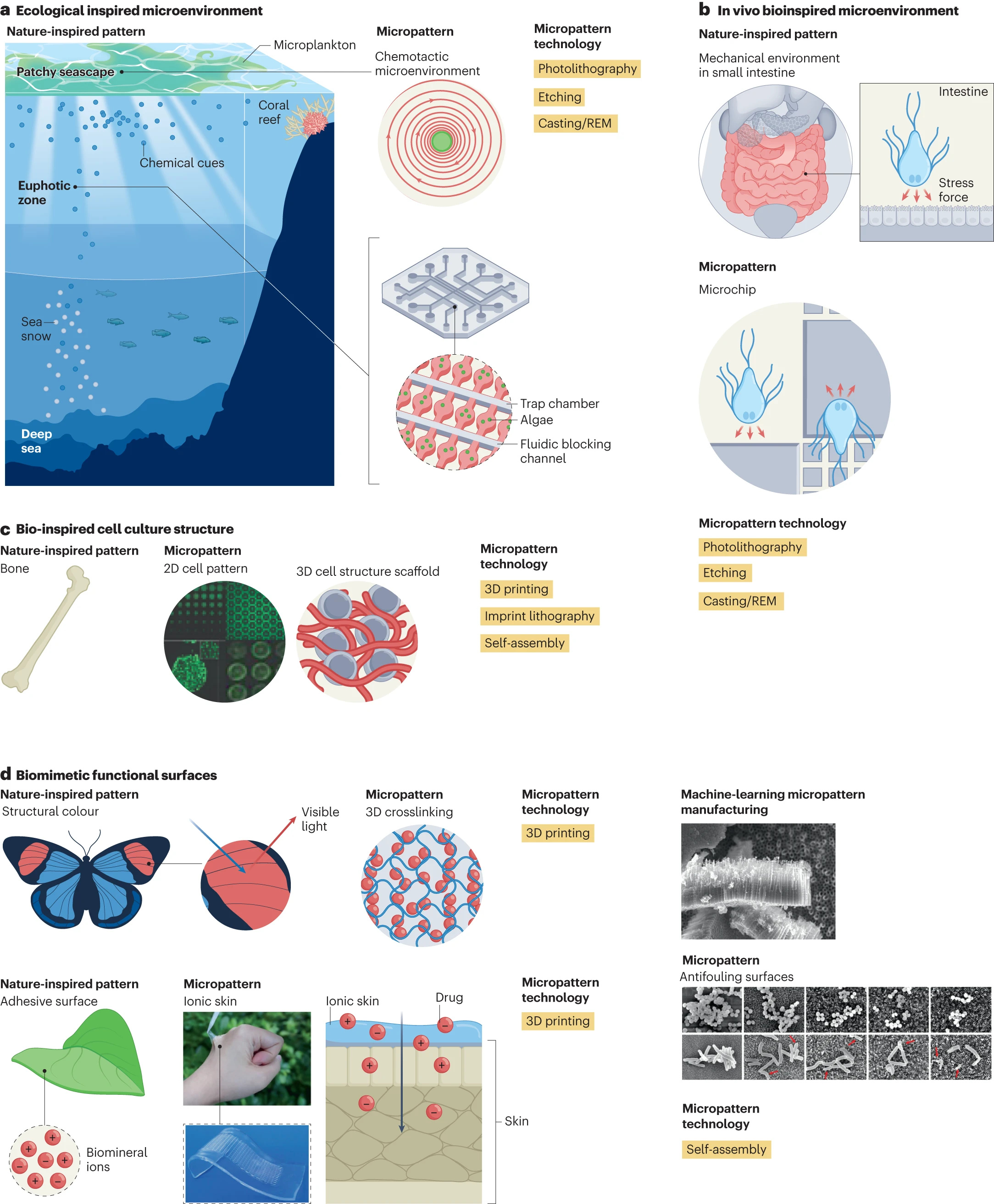 Form factors depend on the intended application. a, Ecological inspired microenvironment, focusing on an ecological microplankton microhabitat in a marine euphotic zone that receives enough light for photosynthesis to occur and induce chemotaxis to supply the food web. b, In vivo bioinspired microenvironment, showing in vivo-like physical microenvironment of the stress force field in the small intestine. c, Nature-inspired micropattern applications mimicking bioinspired cell culture structures, focusing on reconstituting 2D and 3D cell culture scaffolds. The 2D cell patterns show the generation of a heterogeneous microtissue array. The 3D cell culture shows a scaffold-based strategy for bone graft substitutes. d, Nature-inspired micropattern applications mimicking biofunctional surfaces, including adhesive surfaces, antifouling surfaces and structural colour facilitated by 3D-crosslinking. REM, replica moulding. Part b adapted with permission from ref. 42. Copyright 2020 American Chemical Society. Part cadapted with permission from ref. 36. Part d (adhesive surfaces) adapted with permission from ref. 20, Wiley. Part d (antifouling surfaces) adapted with permission from ref. 120.
Principles of nature inspiration proposed by Dr. Xingcai Zhang
There are four key principles of nature inspiration: foundation, nature inspiration, functionality design and efficiency and sustainability.
Foundation
Nature inspiration requires a general understanding of the structure–functionality–manufacturing relationship of materials science, which acts as a synergistic triangle. The structure of a material or micropattern directly impacts its function and manufacture. Meanwhile, the manufacturing processes can influence the structure and functionality of the final product. Similarly, the desired functionality guides material selection and manufacture.
Nature inspiration: self-assembly, hierarchy and function integration
Many natural systems form structures through self-assembly, meaning that they spontaneously organize into complex architectures without external intervention47. This principle can be used to design self-assembled materials and structures for nanotechnology and robotics. Natural and biological systems also have hierarchical organization, with structures and functions occurring at multiple scales, integrating multiple functions into a single structure or system. Mimicking this hierarchical organization enables development of materials with enhanced properties, such as strength, flexibility and self-healing capabilities. For example, bird feathers have hierarchical structures that provide both insulation and flight. The hierarchy is usually formed by self-assembly to achieve function integration. This principle has inspired the design of multifunctional materials and micropatterned devices that can perform multiple tasks simultaneously48.
Nature-inspired functionality design
Natural systems have evolved powerful function integration, sophisticated sensing mechanisms, real-time environmental responses and optimized structures. Understanding how natural and biological systems sense and adapt to challenges, adaptive and responsive materials can be developed.
Efficiency and sustainability
In terms of energy consumption, resource use and overall performance, natural systems are highly efficient. Learning from the efficiency of nature, sustainable and eco-friendly solutions can be developed, which minimize environmental impact to provide sustainable technological advancements.
Nature-inspired micropattern design
A nature-inspired micropattern can be designed using either a bottom-up — starting with a biological model that is adapted to a technical engineering challenge — or top-down approach, in which a technical challenge is identified and an appropriate biological model found.
Usually, the technical challenge is first defined. The key step is to establish a correspondence between the technical problem and potential solution. The biological solution could be found by searching a database, such as AskNature, in which thousands of biological strategies are deposited and categorized by function49. Mechanisms that contribute to the inspired functions should be carefully examined and key features abstracted. As an example, when mimicking an octopus sucker cup, at first only the cup-shaped micropattern was adopted by researchers50. Later, the rim and infundibulum structures were included to form a sucker-like 3D microtip that showed improved performance on underwater surfaces and rough skin51. Eventually, protuberance was introduced and markedly increased the product quality52. Further research suggests that by adjusting the sucker-cup size, a tunable adhesive force can be achieved53. This example demonstrates the importance of identifying all key features and using a comparative method for greater success54.
After identifying a biological strategy, it is then translated to an engineering design to form a prototype. Materials should be carefully selected, considering variables including stiffness, hydrophobicity, permeability, transparency and fabrication technique. Not all structures observed in natural materials can be replicated by currently available materials or fabrication techniques. Sometimes, scalability also needs to be considered, particularly when working on a design intended for mass production. The final step is to test or evaluate the design, including fabrication feasibility and function realization. This step can be supported by computer-aided engineering, the broad use of computer software — such as computational fluid dynamics55, circuit simulation analysis56, finite element analysis and topology optimization57 — to aid analytical engineering tasks. A summary of nature-inspired micropattern design processes and tools is given in refs. 16,58,59, with a representative example in ref. 60.
A machine-learning-based approach can accelerate shape programming of nature-inspired micropatterns and determine their heterogeneity61. Countless natural patterns, materials, geometries and fabrication strategies have been reported using this approach. Each parameter has unique advantages and disadvantages. Artificial intelligence (AI) can be used to systematically understand all possible natural parameters, to help with conceptualization, specification, material choice and fabrication method62.
Material selection
A vast range of materials — including inorganic, organic and nanoparticle materials — has been used to fabricate nature-inspired micropatterns. Material features, such as surface charge, hydrophobicity/hydrophilicity, stiffness, air permeability and biocompatibility, need to be considered according to each application.
Inorganic materials
Silicon and glass are the most used structural inorganic materials for micropatterns. Monocrystalline silicon, a hard semiconductor material, can be patterned by wet or dry etching63,64. Wet etching uses a liquid etchant. Depending on the etchant used, anisotropic or isotropic etching can be achieved. For instance, hydrofluoric acid can be used for isotropic etching and potassium hydroxide for anisotropic etching. During isotropic etching, silicon is etched equally in all directions, resulting in a cavity with rounded corners and edges. In traditional micro-electromechanical systems (MEMS) techniques, silicon is often used to fabricate a micropattern, such as an antireflection surface cone, a lotus leaf micropillar pattern or the foot micropattern of a gecko65. Anisotropic etching of monocrystalline silicon is often used to fabricate high-aspect-ratio microstructures. Glass is a low-cost, amorphous, isotropic and biocompatible material. Often, glass is patterned by wet etching with hydrofluoric acid, but only shallow microstructures are possible with this approach. The silicon or glass surface is hydrophilic and can be made hydrophobic by coating with a self-assembled monolayer. For nature-inspired applications, silicon and glass are frequently used to fabricate moulds to replicate a micropattern, rather than acting as the micropattern themselves66,67.
Metals and alloys — such as nickel, nickel–cobalt and magnesium–lithium — are sometimes used as moulds for hot embossing or microinjection moulding68. Metallic oxides are also used to fabricate moulds. Anodic aluminium oxide (AAO) with micropores or nanopores can be prepared by etching, followed by micropatterning with various shapes — such as a nanofibre, micropillar, microneedle or other shaped tip — and can be replicated in a different material by replica moulding, hot pressing or casting69,70,71.
Organic materials
Various polymers, including thermoplastics, elastomers, resists and hydrogels, have been used to fabricate nature-inspired micropatterns. Thermoplastics become plastic when heated above the glass transition temperature, enabling hot embossing or moulding at elevated temperatures72. The most used thermoplastic materials include poly(methyl methacrylate) (PMMA) and PS. They have modulus at the gigapascal level, enabling a high patterning resolution of <10 nm (ref. 68). The surface properties of PMMA can be modified by appropriate treatment, such as vapour-phase deposition of perfluorodecyltrithoxysilane to generate a hydrophobic PMMA surface71. Other thermoplastics, such as polyvinyl sulfate73 and polyethylene74, are also frequently used75.
PDMS and Ecoflex are among the most used thermo-curable elastomer materials. Both are appropriate for stamping, imprinting, moulding or casting72. PDMS is a hydrophobic elastomer and is widely used in laboratories as it is mechanically strong, optically transparent, flexible, durable, biocompatible, gas-permeable and has high thermal stability. These features make it suitable for biology and life science applications. Linear PDMS can be crosslinked to form an elastomer using an organometallic crosslinking reaction. The stiffness and air permeability of PDMS can be tuned by changing the base to the curing-agent ratio. Usually, PDMS is used to fabricate micrometre-scale features, such as tree-frog toes29,76, gecko feet and petal-effect adhesive surface. Shrinkage and differences in the thermal expansion coefficient of PDMS and the mould may distort replicated nanometre-scale features. Mass production of PDMS is a challenge owing to high fabrication costs77. Ecoflex is a silicone rubber with good biocompatibility and lower adhesion, air permeability, tensile strength and modulus compared with PDMS, which is frequently used to fabricate stretchable structures78,79.
PUA is a transparent, UV-curable material that has low air permeability, is biocompatible, chemically stable, flexible and easy to mould. The modulus is tunable between 20 MPa and 320 MPa by changing the hard-to-soft modulator ratio80,81. PUA can be used to make a stretchable pattern — for example, sucker cups of octopus51,82, gecko pads80,83, microhooks81 and adhesive micropillars — or as a mould for soft lithography. Another frequently used polyurethane-based material is Norland optical adhesive, which is also UV-curable84.
Photoresists are a class of photosensitive resins, including positive resins, which become more soluble in the developer, and negative resins, which crosslink, making them harder to dissolve in the developer. Photoresists are typically used to create a pattern or as a sacrificial layer. SU-8 is an EPON epoxy negative resin dissolved in γ-butyrolactone. The viscosity can be adjusted by changing the polymer-to-solvent ratio to produce a spun-resist layer ranging from 500 nm to 1200 µm, with an aspect ratio that can surpass 18 (ref. 85). SU-8 can be patterned by photolithography and used as mould in casting, embossing or moulding29. Compared with silicon, an SU-8 mould is easier and cheaper to fabricate, but less durable.
Hydrogels are 3D crosslinked hydrophilic polymer networks. They contain large amounts of water, usually 10–20%, and in extreme cases 96%, of the total weight86. The water portion has similar physicochemical properties to liquid water but displays solid-like rheological behaviour87,88. Natural hydrogels can be derived from polysaccharides (alginate and chitin)89, proteins (collagen, gelatin and fibrin)90,91 or extracellular matrix (Matrigel)92. Most are biocompatible, with weak mechanical properties. Modifications can improve their function and properties93. By contrast, synthetic hydrogels — including polycaprolactone; poly(vinyl pyrrolidone); poly(lactic acid); poly(ethylene glycol)94; and poly(vinyl alcohol) — demonstrate improved mechanical properties, with greater control over their physicochemical properties and functions95,96. For nature-inspired applications, hydrogels with excellent biocompatibility, high water content, multiparous structures and tunable softness can be patterned and used to mimic tissue and organ microenvironments97, such as skin20, cartilage98 or tumours. Some hydrogels are stimuli-sensitive and can be patterned by incorporating photo initiators or through UV-light exposure, in a photolithography-like process95,99. Advances in bioprinting have enabled fabrication of more complex cell patterns100. Additionally, hydrogels have been used to modify micropattern surfaces to enhance functions. For example, when designing a gecko-inspired adhesive, a mushroom-shaped PDMS micropattern was modified with poly(dopamine-methacrylamide-co-methoxyethyl-acrylate-co-N-isopropylacryl-amide), which improved the adhesive performance101. Fluoride-containing molecules, such as 1H,1H,2H,2H-perfluorodecyltrimethoxysilane, are typically used to modify the pattern surface, particularly to facilitate mould release102.
Micropattern fabrication
Nature-inspired micropatterns control the spatial distribution of materials to replicate biophysical, biochemical or geochemical features that appear in natural systems. Typically, these features are configured as microchannels or pattern arrays on a substrate (2D) or 3D microstructure and range in size from nanometres to micrometres. Many microfabrication techniques are used to develop nature-inspired micropatterns. These methods can be divided into three groups, derived from the semiconductor industry, the moulding industry and other advanced manufacturing technologies.
Photolithography and etching
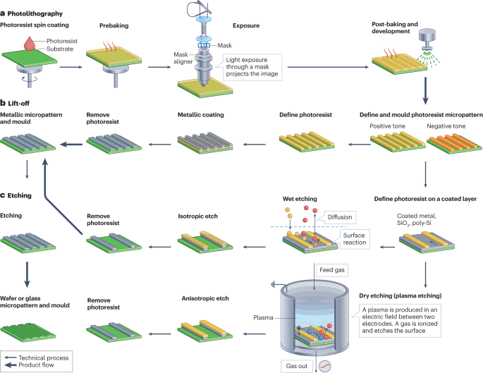
Photolithography and etching not only derive from a standard MEMS technique and are widely used in the semiconductor industry but also enable preparation of micropatterned surfaces, microfluidics, nanostructures and nanoparticles. The process can be split into one or more cycles, each containing three steps: thin film coating, photolithography and etching. Using this approach, micrographics can be precisely transferred from a lithography mask to a substrate surface (Fig. 1).
The operation can be split into one or more cycles of photolithography, thin-film coating, lift-off and etching to achieve precise transfer of micrographics from a lithography mask onto a substrate surface. a, The final product of photolithography is a copy of the photomask micropattern, formed by resist polymer that remains on the substrate. It could be used as a mould for soft lithography or to define a pattern on a substrate during subsequent processing steps. b, Lift-off is used to pattern metal, dielectric or polymer films. c, Etching is used to create micropatterns on a substrate, such as a silicon wafer or glass slide. It can be divided into two categories, depending on the method used to remove unprotected materials: wet etching, using a chemical solution as an etchant, and dry etching, using gas or ions as an etchant. Thin arrows indicate the direction of a technical process and thick arrows indicate a product flow.
Photolithography images a structure written in a lithographic mask onto a light-sensitive resist and photosensitive or photo-curable material deposited on a substrate. The photosensitive resist and material character— for instance, positive or negative, sidewall morphology, defect and resistance — are vital to the success of subsequent steps. First, the photoresist is spin-coated on the substrate. By changing the resist viscosity and spin-coating speed, the thickness of the photoresist can be tuned. The coated substrate is then exposed to UV light and a lithographic mask defines the exposure areas. The substrate is treated by a development process to remove any unwanted resist. For a positive photoresist, the exposed areas are removed, whereas for a negative photoresist, exposed areas remain and unexposed areas are removed. The final product is a copy of the photomask micropattern, formed by the resist polymer on the substrate81,103,104 (Fig. 1a). The size of features created using this approach ranges from several micrometres to hundreds of micrometres. Formed micropatterns may be used as a mould for soft lithography or to define a substrate pattern in subsequent processing by lift-off and etching. Variants of photolithography have been developed by changing the light source — X-rays, electrons or ions — to achieve higher resolution. These variants can be used to create micropatterns at the nanometre scale.
Lift-off is an additive transfer technique used to pattern metal, dielectric or polymer films in the micrometre-to-sub-micrometre range. A positive resist pattern is used as a sacrificial layer. It is first formed on the substrate by lithography. Material to be transferred is then deposited as a thin film, keeping the film on the top of the sacrificial layer pattern or in the gap of the pattern. Then, the substrate is exposed to UV light. The sacrificial pattern and deposited material film on it are removed, leaving the desired material in the gap of the pattern (Fig. 1b). To completely remove the resist/material pattern, the positive resist should be three times thicker than the deposited material. This approach is typically used to produce thin-film patterns and is not suitable for thick patterns. Lift-off is used when the coating material cannot be etched. A modified lift-off method was used to generate a cell array for investigating cell behaviour81,105,106. In the one lift-off method, a film with cracks from mechanical failure was used as a sacrificial layer to produce nanowire patterns107.
Etching is a subtractive pattern transfer technique, which involves removing the material from a specified area. The etching process can be isotropic or anisotropic. In isotropic etching, both the vertical and lateral etch rates are comparable, leading to micropattern expansion or rounded corners. During anisotropic etching, the etch rate in the downward direction is faster than the sideways directions. Cavities with straight sides can be produced, making it possible to precisely define the micropattern structure. Etching starts with a photoresist coating and a definition of the micropattern on the substrate. Any material not protected by the photoresist is removed in the etching process (Fig. 1c). Depending on how the unprotected material is removed, etching can be divided into wet or dry etching69,70,71,108. Wet etching uses chemical solutions to react with the substrate and remove materials, usually resulting in isotropic and rough surfaces. As a result, it is not suitable for fabricating high-resolution and high-dimensionally accurate micropatterns109,110,111. Dry etching uses gases or ions as an etchant and includes physical, chemical and physical–chemical dry etching. Physical dry etching uses high-energy particles, such as an ion or electron beam, to remove the material. It can be applied to nearly all materials, with relatively low etching rate. Chemical dry etching uses a chemical etchant gas to react with the substrate. Consequently, the process is highly material-selective and, similar to wet etching, results in an isotropic etch. Physical–chemical dry etching uses reactive ions or plasma, giving an anisotropic etch and relatively high aspect ratio31,60,112,113.
When fabricating a nature-inspired micropattern, etching is often used to create a micropattern on a substrate, such as a silicon wafer or glass slide. The resulting product can either be used as a stand-alone micropattern or as a mould for another patterning technique, such as casting, moulding or hot embossing67,68,69. Etching may also be used to develop new micropattern fabrication techniques. For example, in selective etching, the material can be rolled into a nanotube with precisely controlled wall thicknesses, at the scale of a single atomic layer114.
Soft lithography
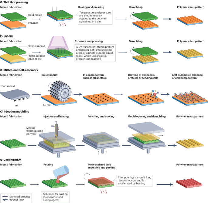
Soft lithography includes techniques developed in the traditional moulding industry — hot embossing, injection moulding and casting — performed at finer dimensions, down to the nanometre scale115,116. These techniques are widely used to create structural patterned surfaces or coatings with specific biomolecules. They start by creating a mould or stamp with the opposite geometry to the desired micropattern by photolithography or another MEMS technique. Mould surfaces are often modified with a non-stick layer, such as perfluorodecyltrithoxysilane, to facilitate release. Desired polymer micropatterns are then replicated from the moulds or stamps (Fig. 2). Soft lithography has advantages over other lithography techniques. For example, although moulds are fabricated in clean room and have a relatively high cost, soft lithography can be performed in an ordinary environment. Additionally, moulds and stamps are reusable, reducing the overall fabrication cost. Soft lithography techniques for nature-inspired micropatterns include nano-imprinting lithography (NIL), casting or replica moulding (REM) and microinjection moulding.
Soft lithography usually starts by creating a mould or stamp with the geometry opposite to the desired micropattern using photolithography or another micro-electromechanical technique. A soft material, such as a melted metal, thermoplastic or curable material, fills a die and replicates the desired micropatterns by thermal nano-imprinting lithography (TNIL) and hot embossing (part a); ultraviolet NIL (UV-NIL) (part b); microcontact NIL (MCNIL) and self-assembly (part c); injection moulding (part d); or casting and replica moulding (REM) (part e). Thin arrows indicate the direction of a technical process and thick arrows indicate a product flow.
Follow the Topic
-
Nature Reviews Methods Primers
An online-only journal publishing high-quality Primer articles covering analytical, applied, statistical, theoretical and computational methods used in the life and physical sciences.



Please sign in or register for FREE
If you are a registered user on Research Communities by Springer Nature, please sign in