Solution Processed Kesterite Solar Module with 10.1% Certified Efficiency
Solution processing is the great advantage for emerging thin film solar cells, which has demonstrated success in organic and hybrid perovskite solar cells. Kesterite structured Cu2ZnSn(S,Se)4 (CZTSSe) has emerged as a highly promising green thin-film technology due to its eco-friendly elemental composition, high theoretical efficiency, and high absorption coefficient. However, unlike the relatively straightforward formation of organic or perovskite thin films during solvent evaporation, the solution-based fabrication of multi-element CZTSSe thin film involves two critical steps: precursor deposition and high-temperature crystallization (selenization). This seemingly clear pathway conceals a significant pitfall that multiphase fusion reactions easily cause compositional inhomogeneity and electronic property fluctuations in the film, becoming a barrier to efficiency enhancement and industrialization of CZTSSe solar cells.
We have made a breakthrough in achieving direct phase transformation crystallization based on Cu+-Sn4+ solution method (Figure 1a), pushing CZTSSe solar cell efficiency to 13% after almost a decade stagnation in 12.6%, however, we encountered a setback at the critical step towards practical application of manufacturing uniform and reproducible large-area solar module. The efficiency of our first fabricated CZTSSe module was only 4.3%, with a staggering cell-to-module power conversion efficiency (CTMPCE) loss of 56.81%, which reveals a hard truth that the success of highly efficient small-area cells in the lab is far from equivalent to producing high-quality large-scale absorber films.
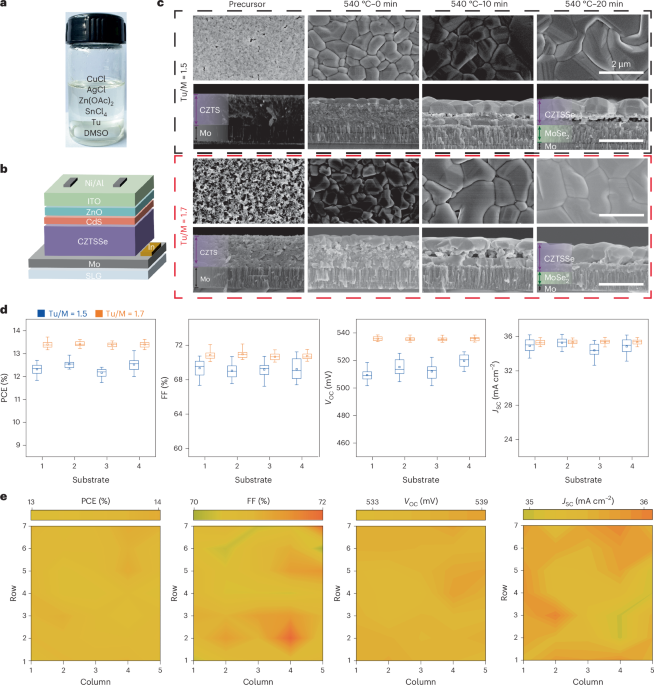
We further embarked on an in-depth exploration for the large cell-to-module loss. Through the characterization and analysis of the film morphology and element distribution during different stage of crystallization process, a key issue emerged: during the early stage of the selenization, a dense crystalline layer already forms on the surface of the film, which acts as an invisible barrier as a hard shell and seriously hinders the subsequent penetration of selenium vapor into the interior of the film. This hinders the grain growth in the vertical direction and results in poor film uniformity and high surface roughness (Figure 1c). The nonuniform absorber film cannot support the manufacturing of efficient and large-area devices, accounting for the poor performance and large CTM loss of our previous modules.
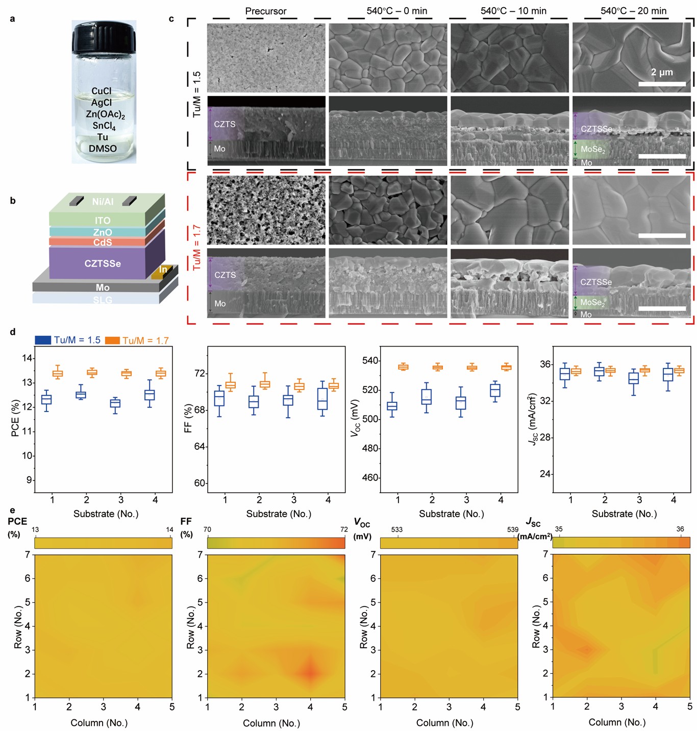
Figure 1. The uniformity of solution processed kesterite solar cells. (a) Picture of the precursor solution. (b) Illustration of the kesterite solar cell with a configuration of SLG/Mo/CZTSSe/CdS/ZnO/ITO/Ni/Al. (c) Top-view and cross-sectional SEM images of the precursor and absorber films with Tu/M ratio of 1.5 (Tu1.5) and 1.7 (Tu1.7) at different stage of the grain growth (selenization). (d) Plots of the statistical photovoltaic parameters (PCE, FF, VOC, and JSC) of Tu1.5 and Tu1.7 solar cells. Total 140 devices on 4 substrates (each contains 35 devices) fabricated in one batch are included for each condition. The box plot denotes median (center line), mean value (dot), 25th (bottom edge of the box), 75th (top edge of the box), 95th (upper whisker) and 5th (lower whisker) percentiles. (e) Contour plots of device parameter distribution of 35 cells on one substrate for Tu1.7.
The issue has been identified, but how to solve it? If we could change the microstructure of the precursor film and regulate its porosity so that to prevent the rapid formation of a dense top layer at the early stage of the selenization and create more space for subsequent Se permeation and more time for lateral grain growth, we might be unable to improve film uniformity. The microstructure of the precursor film is closely linked to the composition of the precursor solution. Thiourea (Tu) is the organic precursor and S source in the precursor solution, which decomposes during thermal decomposition and releases volatile gases from the film, the direct drive for the film porosity. Therefore, we systematically regulate the ratio of Tu to metal ions in precursor solution and investigate the film morphology. The results were encouraging: after increasing the Tu content, the precursor film became more porous and looser, enabling the formation of a looser top crystalline layer at an early stage of the selenization, which allows more Se to penetrate into the film bulk and provides more room for lateral grain growth and eventually improving the uniformity and surface flatness of CZTSSe absorber film (Figure 1c).
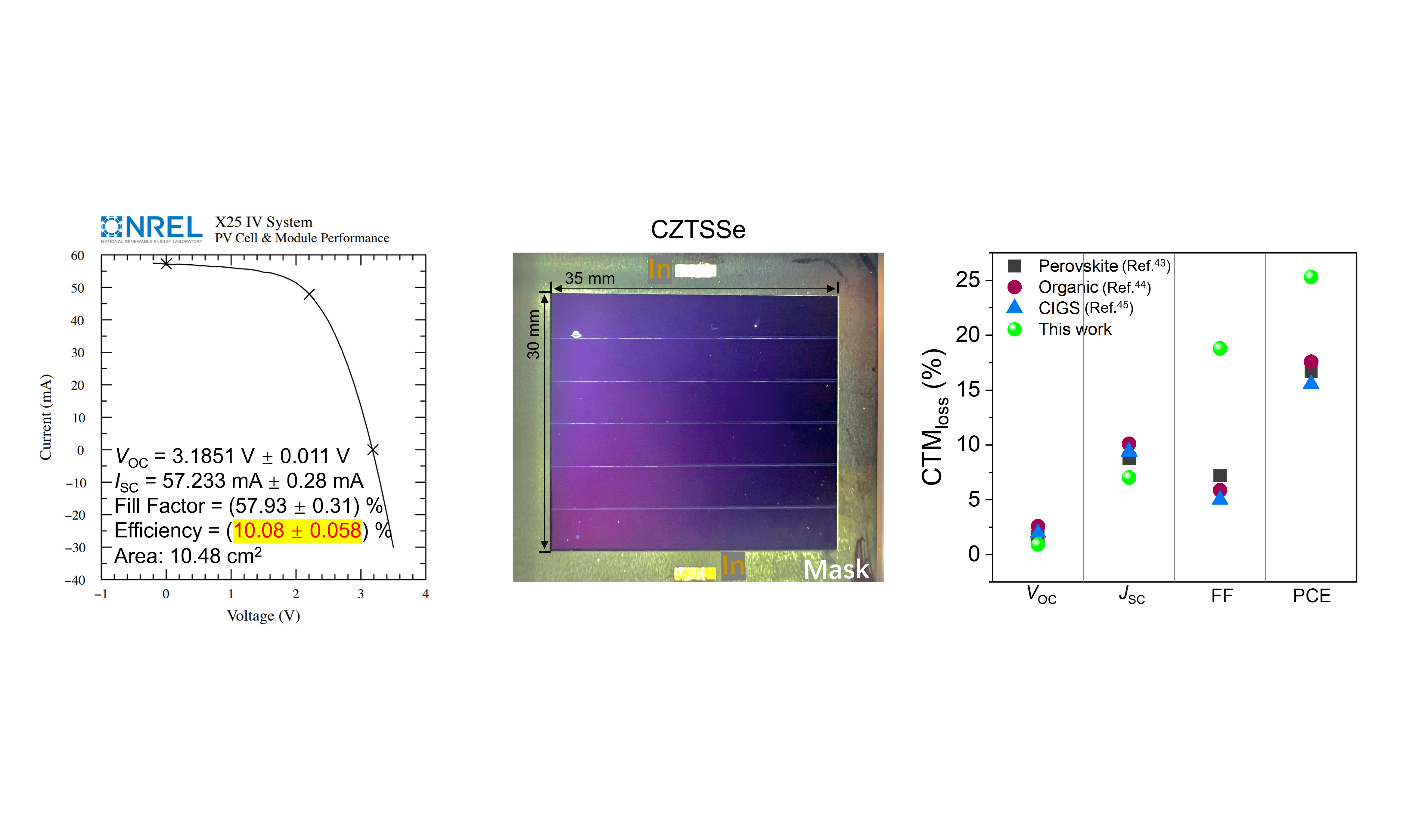
Figure 2. kesterite module structure modification and cell to module (CTM) losses. (a) Cartoon of the module structure and structure modification (SM). The black dotted line is the flow of the current. (b) The I-V curves of the primary module without (M) and with antireflective coating (M-ARC), module after structure modification without (M-SM) and with ARC (M-SM-ARC). (c) The I-V curve of the NREL-certified 10.08% efficient kesterite module. (d) Picture of the obverse side of the certified module. The area is defined by the mask. (e) Comparison of the CTM losses of the emerging thin film solar modules (Perovskite, Organic, and CIGS).
Based on the improved uniformity of the absorber film, we successfully achieved an average efficiency of 13.4% for single-cells (active area of 0.1 cm2) with very low standard deviation (Figure 1d) and 8.91% efficiency solar module. But this was not the end. We had further modified the module structure to reduce non-ideal contact and shunting caused series resistance, resulting in a certified 10.1% efficient (National Renewable Energy Laboratory, NREL) solar module (with an aperture area of 10.48 cm2) with a low CTMPCE of 25.3% and the lowest CTM loss in VOC (0.93%) and JSC (7.03%) among state-of-the-art emerging thin-film solar modules (Figure 2).
This is not only the first record efficiency solution-processed CZTSSe module, but also a journey for understanding and tackling the underlying challenges in fabrication of inorganic thin films via solution approach. This work provides a clear and feasible technical pathway for solution-processing of high-performance large-area inorganic compound thin-film solar cells and modules.
Follow the Topic
-
Nature Energy
Publishing monthly, this journal is dedicated to exploring all aspects of this on-going discussion, from the generation and storage of energy, to its distribution and management, the needs and demands of the different actors, and the impacts that energy technologies and policies have on societies.


Please sign in or register for FREE
If you are a registered user on Research Communities by Springer Nature, please sign in