Wafer-scale low-cost complementary vertically coupled plasmonic structure for surface-enhanced infrared absorption
Published in Electrical & Electronic Engineering
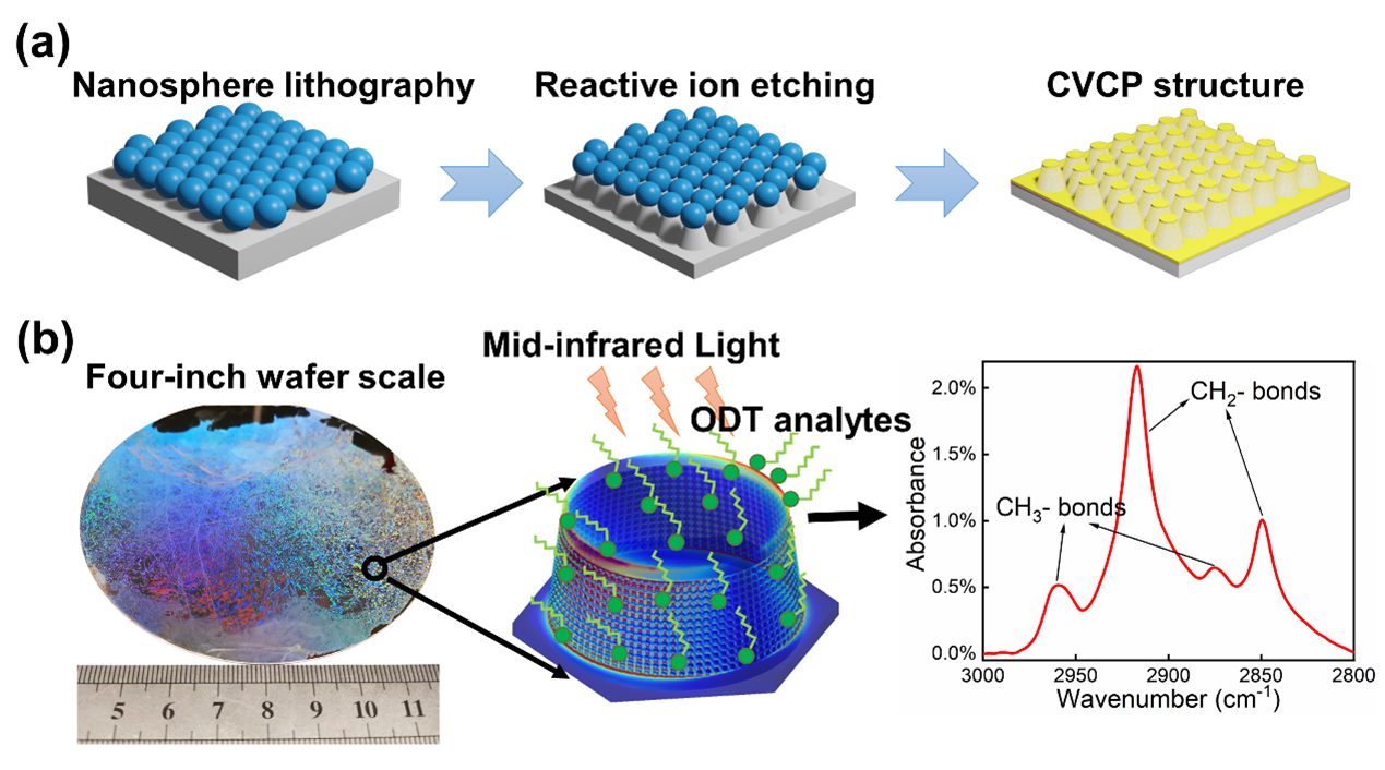
In this article, we reported a scalable nanofabrication approach for the hexagonal packed complementary vertically coupled plasmonic (CVCP) structures in surface-enhanced infrared absorption (SEIRA) applications. This fabrication approach consists of nanosphere lithography, reactive ion etching, and metal deposition and can be implemented on a four-inch wafer scale with low cost and high uniformity. The CVCP structure contains dense plasmonic nanoparticles inside a three-dimensional cavity nanoantenna array. The localized surface plasmon resonance between the top-bottom metallic nanoantenna couple generates a solid localized electric field inside the cavity. A high simulated and experimental SEIRA electric-field enhancement was achieved by optimizing the height of the silicon nanopedestals. Using a representative monolayer octadecanethiol, an enhancement factor of 2.1 × 10³ was demonstrated with an optimized structure geometry. When the detection area was extended to square millimeters, the limit of detection of monolayer octadecanethiol on the CVCP substrate reached 10 nM, which is four orders of magnitude lower than that on a flat gold substrate. This study demonstrates a feasible fabrication approach for producing three-dimensional nanoantenna structures with high enhancement factors in a scalable fashion, empowering the practical application of SEIRA substrates.

Surface-enhanced infrared absorption (SEIRA), which is based on the interaction between photons and valence bonds, is a powerful technique for analyzing chemical components and holds promise for applications in disease diagnosis, industrial production, and environmental conservation. Because the vibration frequencies of crucial chemical functional groups and the skeleton of molecules fall within the 4000–1500 cm-1 wavenumber region, this region is called the functional group region. The absorption rates are extremely weak in this waveband because the molecular size is 3–4 orders of magnitude smaller than the wavelength of light and the absorption cross-sections are very small (10-20 cm2 per molecule). To enhance the interaction between incident light and analyte molecules, the plasmonic effect has been employed as an effective approach to constrain light to subwavelength scales, usually tens to hundreds of nanometers. The electromagnetic enhancement provided by plasmonic focusing is scaled as the square of the incident field strength, as denoted by |Eω|2. When analytes are loaded onto the SEIRA structure, the plasmonic oscillation empowers strong coupling between the electromagnetic fields and the molecular vibration of the analytes. The signal strengths of the analytes in this harmonic resonance process can be enhanced by several orders of magnitude. Multiple nanoantenna shapes, such as nanorods, nanofans, split rings, and nanogaps, have been produced to achieve efficient enhancements. These metallic nanostructures concentrate light into an extremely small volume, typically at the end of the nanotip or inside a tiny nanogap, resulting in a significant enhancement of the local electric field, typically up to 105.
However, SEIRA requires the collection of light from a macroscopic area, and therefore demands a high proportion of hotspots and largearea fabrication of nanoscale plasmonic structures. The absorption intensity obtained during SEIRA measurements represents the average intensity over the entire area with different electric field enhancements. Therefore, the maximal electric field and hotspot area determine the final absorption intensity. Additionally, because the feature size of a single SEIRA structure is submicron and sometimes even several nanometers, normal ultraviolet lithography is not possible; therefore, nanolithography, such as electron-beam lithography, is usually required. Throughput and cost limit the large-area and low-cost fabrication of SEIRA structures.
To overcome the aforementioned challenges, researchers designed an equally distributed nanoantenna using laser interference lithography to fabricate a relatively larger SEIRA substrate area of approximately 1cm2. These SEIRA substrates generated denser hotspots with enhancement factors (EFs) as large as 104. However, these laser-based fabrication methods are inefficient in terms of cost and sample size. Alternatively, nanosphere lithography, self-assembly or chemical etching methods have been employed to produce metallic nanostructures on a large scale and at low cost, but they usually suffer from low signal EFs, usually below 102, owing to their non-uniform distribution and limited structural choices. For example, nanosphere lithography usually employs colloidal nanospheres as templates to produce triangular metallic nanostructures using the lift-off method or to prepare metal split-rings using the oblique evaporation method. However, these single-layer metal structures either have a small hotspot proportion or are unevenly distributed during fabrication, resulting in a modest enhancement of the final signal. In summary, fabrication approaches that balance fabrication efficiency and device performance are required to facilitate the practical application of SEIRA technologies.
The aforementioned two-dimensional nanoantenna structures have relatively small modal volumes owing to the typically low surface-tovolume density ratio of plasmonic hotspots in nanostructures. To enhance the interaction between analytes and mid-infrared light, three dimensional (3D) nanoantenna structures have been explored, including 3D nanoporous gold antennas. 3D nanoparticle supercrystals, and double-layered metal structures. These 3D nano structures provide a simple method for obtaining a high proportion of hotspot areas with a high surface-to-volume structure. However, these studies have not investigated the use of hybrid plasmonic and optical cavity structures to enhance the SEIRA performance. Furthermore, it is still challenging to realize the large-area fabrication of these 3D plasmonic structures.
Herein, a hexagonal packed complementary vertically coupled plasmonic (CVCP) structure fabricated using nanospherical lithography is reported. In this CVCPstructure, the metallic nanostructures at the top and bottom of the silicon nanopedestal structure can generate localized surface plasmon resonance (LSPR) and vertically couple to each other inside the 3D cavity. Moreover, the densely assembled metallic nanoparticles on the sidewall of the silicon nanopedestal can further strengthen this coupling, generating a stronger electric field intensity and larger proportion of hotspots. By combining hybrid plasmonic and optical cavities, the developed structure generates a tightly confined electric field spatial distribution, leading to a high electric field enhancement. Moreover, this CVCP structure, as compared to previously reported 3D structures, can be reliably fabricated in a scalable fashion, thus ensuring highly stable and predictable optical properties.
By employing nanosphere lithography to fabricate this structure, the area of the SEIRA substrate could be extended to a four-inch wafer scale with high uniformity. To demonstrate a prototype, self-assembled monolayer octadecanethiol (ODT; CH3(CH2)17SH) was chosen as the test analyte to illustrate the high efficiency of the SEIRA substrate. By adjusting the height of the structure to maximize the electric field coupling, the EF of the detected signal in the ODT reached 2.1 × 10³. After extending the area of measurement to square millimeters, the SEIRA substrate enhanced the detection limit of ODT to 10nM and exhibited a detection limit four orders of magnitude lower than that of a flat gold substrate.
ODT is a molecule that can self-assemble on gold substrates as a monomolecular layer via sulfur-gold bonds and was employed as a standard molecule to demonstrate the SEIRA effect. The CH 2- bonds inside the ODT molecule have symmetric and antisymmetric absorption peaks with wavenumber ranges of approximately 2850–2863 cm-1 and 2916–2936 cm-1, respectively. An FTIR with a microscopehaving a light spot area of 100 × 100 μm was employed to measure the mid-infrared absorption of the analyte. Because the thickness of an ODT monolayer is only 2.5nm, 1400 times smaller than the incident wavelength (approximately 3.5 μm), the interaction between the molecule and light is small and negligible. The experimental results show that the absorption of a monolayer of ODT generated on a bare gold substrate at this concentration is below the detection limit of the detector, as shown in Fig. S4. Next, the same test was performed on a CVCP substrate at a wavelength of 600nm. In this structure, the resonance wavelength was near the absorption peaks of the CH 2- bonds, which is conducive to the enhancement of the mid-infrared absorption.
Sensors and Actuators B: Chemical, Volume 382, 1 May 2023, 133560
Prof. Yang Xu is an IEEE NTC Distinguished Lecturer, Fellow of the Institute of Physics (FInstP), Fellow of Institute of Engineering and Technology (FIET), Fellow of Royal Society of Chemistry (FRSC), Fellow of the Institute of Materials, Minerals and Mining (FIMMM), and IEEE Senior Member of the Electron Devices Society. He received his B.S. degree in Institute of Microelectronics at Department of ECE from Tsinghua University, M.S. and Ph.D. degrees in ECE from the University of Illinois Urbana-Champaign (UIUC), USA. He is now a full professor at the School of Micro-Nano Electronics, Zhejiang University, China. He was also a visiting by-Fellow of Churchill College at the University of Cambridge, UK, and a visiting professor at the University of California Los Angles (UCLA). He has published more than 120 papers including Nature Nanotechnology, Nature Electronics, Nature Photonics, Chemical Reviews, Advanced Materials, Chemical Society Reviews, Nature Communications, Nano Letters, ACS Nano, and IEDM,etc. He holds over 30 granted patents and gave more than 50 talks in international conferences. He is also served as Associate Editor of IEEE T-ED, Photonics Research, and IEEE Nanotechnology Magazine, Editorial board member of IOP Nanotechnology, Microelectronics Journal, Micro & Nano Letters, and IET Circuits, Devices & Systems, Advisory Panel Member of IOP Nanotechnology, and was TPC committee members of IEEE-EDTM, IEEE-IPFA, and IEEE-EDAPS conferences. His research interests include emerging 2D/3D integrated optoelectronic devices for Internet-of-Things and Post-Moore Ubiquitous Electronics.


Please sign in or register for FREE
If you are a registered user on Research Communities by Springer Nature, please sign in