Chipping away roadblocks to commercialisation of higher efficiency silicon heterojunction technology
Published in Electrical & Electronic Engineering

Silicon heterojunction (SHJ) technology is a promising next-generation commercial crystalline silicon (c-Si) photovoltaic technology, due to its high power conversion efficiency (PCE), lean and low-temperature processing, low temperature coefficient and high bifaciality1,2. To date, the PCE of front-back contacted and interdigitated-back contacted SHJ solar cells has reached 26.8% and 26.7%, respectively, setting the world record for single-junction c-Si solar cells3,4. However, the commercial success of SHJ technology remains impeded by challenges in the cost-effective translation of demonstrated small-scale processes to a production environment. Of particular concern, is the uniform and cost-effective deposition of window layers which can reduce parasitic absorption on industrial wafers and low-cost, reliable metallization. Our paper addresses each of these two key commercialisation challenges by presenting technological advances in large area plasma-enhanced chemical vapor deposition (PECVD) technology by Suzhou Maxwell Technologies Co. Ltd (Maxwell) and copper plated metallisation by Sundrive Solar Pty Ltd (SunDrive).
The first challenge is addressed by demonstrating that high PCEs can be obtained on industrial wafers using large-area PECVD chambers with VHF excitation frequencies to deposit nc-SiOx:H window layers on M6-size SHJ cells. Use of nc-SiOx:H layers can reduce the parasitic absorption in the passivating contact layers enabling higher short-circuit current densities (Jsc) and fill factor (FF), however the use of VHF excitation frequencies to achieve crystallisation of the doped window layers has in the past required the use of small PECVD chambers to avoid poor uniformity of deposited films due to standing wave effects. We show that these standing wave effects can be effectively minimised in a production-scale chamber with VHF excitation of 27 MHz to deposit a nc-SiOx:H(n) window layer resulting in a PCE of 25.98% (Fig. 1b) on an M6-size SHJ cell with transition-metal doped indium oxide transparent electrodes on both sides (see Fig. 1a). Comparative SHJ cells produced with (doped) hydrogenated amorphous silicon (a-Si:H) films deposited in a PECVD chamber with the more commonly used RF (13.56 MHz) plasma excitation had a lower PCE of 25.83%.
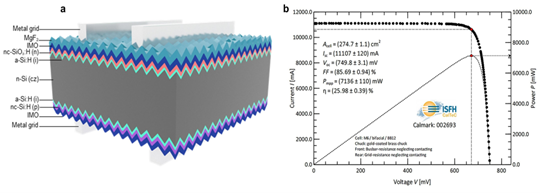 Figure 1. (a) Schematic of a rear-junction SHJ solar cell featuring a frontside nc-SiOx:H(n) window layer as an electron collector; (b) certified I-V curve of the best device featuring a nc-SiOx:H(n) window layer deposited under VHF excitation with screen-printed silver electrodes.
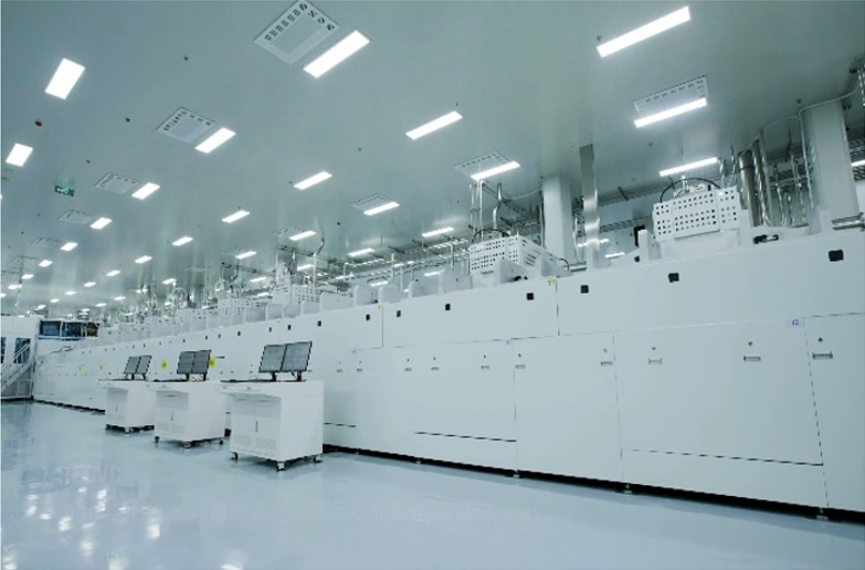
Based on this achievement, Maxwell have successfully designed and developed a large-size PECVD chamber (2.03 m x 2.03 m) under 27 MHz (VHF) excitation for mass production (see Fig. 2a). The industrial equipment enables the loading of 162pcs of half cut M12 wafers (210 mm) in one batch, which corresponds to a throughput of 7200 pieces/h and an annual production capacity of ~ 600 MW. The availability of this new PECVD capability can enable manufacturers to produce industrial SHJ cells at scale with doped hydrogenated nanocrystalline silicon (nc-Si:H) (see Fig. 2b), or its alloys with oxygen (nc-SiOx:H) and carbon (nc-SiC:H), window layers thereby achieving PCEs which have previously only been possible on small-scale lab-based equipment.
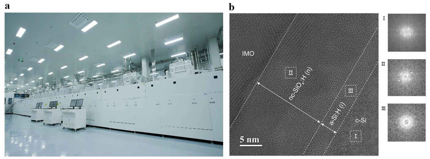
Figure 2. (a) Photo of Maxwell’s large area PECVD/VHF deposition tool; (b) cross-sectional TEM image showing a nc-SiOx:H(n) window layer on a textured SHJ solar cell.
Our paper also demonstrates a viable path to lower cost metallization for SHJ cells. Currently, the screen-printing of silver on both surfaces of front and back contacted SHJ cells comprises 9% of the solar cell cost.5 We report the application of SunDrive’s direct copper plating to replace the screen-printed silver electrode of SHJ cells which can reduce the material costs of the cell by up to 8%.6 Direct copper plating avoids the complexity associated with depositing a seed layer for electroplating and then having to remove the unwanted metal by etching once the copper electrode has been formed.
In addition to reducing the cost of the metallization, SunDrive’s direct copper plating process significantly increased the Jsc and FF from comparative screen printed silver SHJ cells, resulting in a certified world-record PCE of 26.41% for c-Si solar cells with plated copper electrodes (Fig. 3a). The Jsc improvement (0.35 mA/cm2) arises from reduced shading loss, due to a narrow copper finger widths (~ 9 µm), as demonstrated by the cross-sectional SEM image in Fig. 3b. The higher FF results from the polycrystalline plated copper fingers forming an intimate low resistance contact with the transition metal oxide on the textured c-Si surface and the low bulk resistivity of the copper fingers. Modules comprising soldered copper-plated cells show comparable degradation (< 4%) to screen-printed silver SHJ modules after 1000 hrs of damp heat testing indicating that the copper metallization process is durable. Since publication of our Nature Energy article, Maxwell and SunDrive have further improved the efficiency of M6-sized SHJ cells based on the abovementioned technologies to 26.60%.
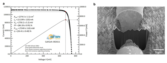
Figure 3. (a) Certified I-V curve of the champion SHJ device with a plated copper electrode under standard test conditions; and (b) cross-sectional SEM image of a plated copper finger on textured c-Si surface.
Our successful demonstration of the integration of high-performance nc-SiOx:H window layers with large-area uniformity and low-cost, performance-enhancing copper plating on SHJ solar cells fabricated on industrial wafers can ‘chip-away’ at roadblocks to large-scale commercialisation of SHJ technology and enable the technology to present a viable alternative for next generation higher efficiency silicon PV technology.
References
- Ballif, C., Haug, F.-J., Boccard, M., Verlinden, P. J. & Hahn, G. Status and perspectives of crystalline silicon photovoltaics in research and industry. Nat Rev Mater 7, 597–616 (2022).
- Green, M. A. Silicon solar cells step up. Nat Energy 8, 783–784 (2023).
- Lin, H. et al. Silicon heterojunction solar cells with up to 26.81% efficiency achieved by electrically optimized nanocrystalline-silicon hole contact layers. Nat Energy 8, 789–799 (2023).
- Yoshikawa, K. et al. Exceeding conversion efficiency of 26% by heterojunction interdigitated back contact solar cell with thin film Si technology. Solar Energy Materials and Solar Cells 173, 37–42 (2017).
- Assuming a silver paste price of US$1,063/kg (based on Q1 2023 data), 18 mg of silver paste per W of 12 BB M12 SHJ cell with a cost of 21 US cents per W.
- Assuming a copper price of US$8.03/kg
Follow the Topic
-
Nature Energy
Publishing monthly, this journal is dedicated to exploring all aspects of this on-going discussion, from the generation and storage of energy, to its distribution and management, the needs and demands of the different actors, and the impacts that energy technologies and policies have on societies.

Related Collections
With Collections, you can get published faster and increase your visibility.
Microgrids and Distributed Energy Systems
Publishing Model: Hybrid
Deadline: Jun 30, 2026


Please sign in or register for FREE
If you are a registered user on Research Communities by Springer Nature, please sign in