Scanning probe microscopy for advanced nanoelectronics
Published in Electrical & Electronic Engineering
The first SPM was invented in 1981 at IBM laboratories in Zurich by Gerd Binnig and Heinrich Rohrer [1], a development that granted them the Nobel Prize in Physics in 1986. That technique was called scanning tunneling microscopy (STM), and consisted on using an ultra-sharp and conductive tip to scan the surface of a conductive sample when the distance between them was few nanometers. The tip-sample distance could be controlled by applying a potential difference between them and measuring the current — which can be converted into distance. Using this technique the shape of molecules and even the position of single atoms could be clearly mapped.
Just one year later, the inventors of the STM had the idea of placing the ultra-sharp tip at the end of a cantilever, which allowed them detecting the tip-sample distance by monitoring its bending using an optical system — both tip and sample do not need to be conductive [2]. This technique, called atomic force microscopy (AFM), represented a complete revolution in different fields of nanoscience because it allowed using the ultra-sharp tip to monitor other different magnitudes during the scan (simultaneously to the tip-sample distance). Consequently, 1993 Sean O’Shea and co-workers at University of Cambridge used an AFM provided with a conductive tip and a source-meter to monitor the topography and the conductivity of a SiO2 sample [3]. This technique was called conductive AFM, and initially it was used to characterize (at the nanoscale) multiple phenomena of thin dielectric films, such as tunneling current [4-6], polycrystallization [7-9], charge trapping and de-trapping [10-11], random telegraph noise [12-13], stress induced leakage current (SILC) [14], dielectric breakdown, and it can also distinguish which locations within the dielectric film promote RS [15-19], as well as what are the properties of the conductive filaments [20-21]. After the invention of the CAFM, many other similar SPM-based techniques were developed in order to measure capacitance, contact potential difference, piezoelectricity, flexoelectricity, and photoelectricity (among many others) [22]. Furthermore, the tip of the SPM has been also used to carry out local material modification, patterning and nanolithography, allowing nanofabrication of different structures and devices.
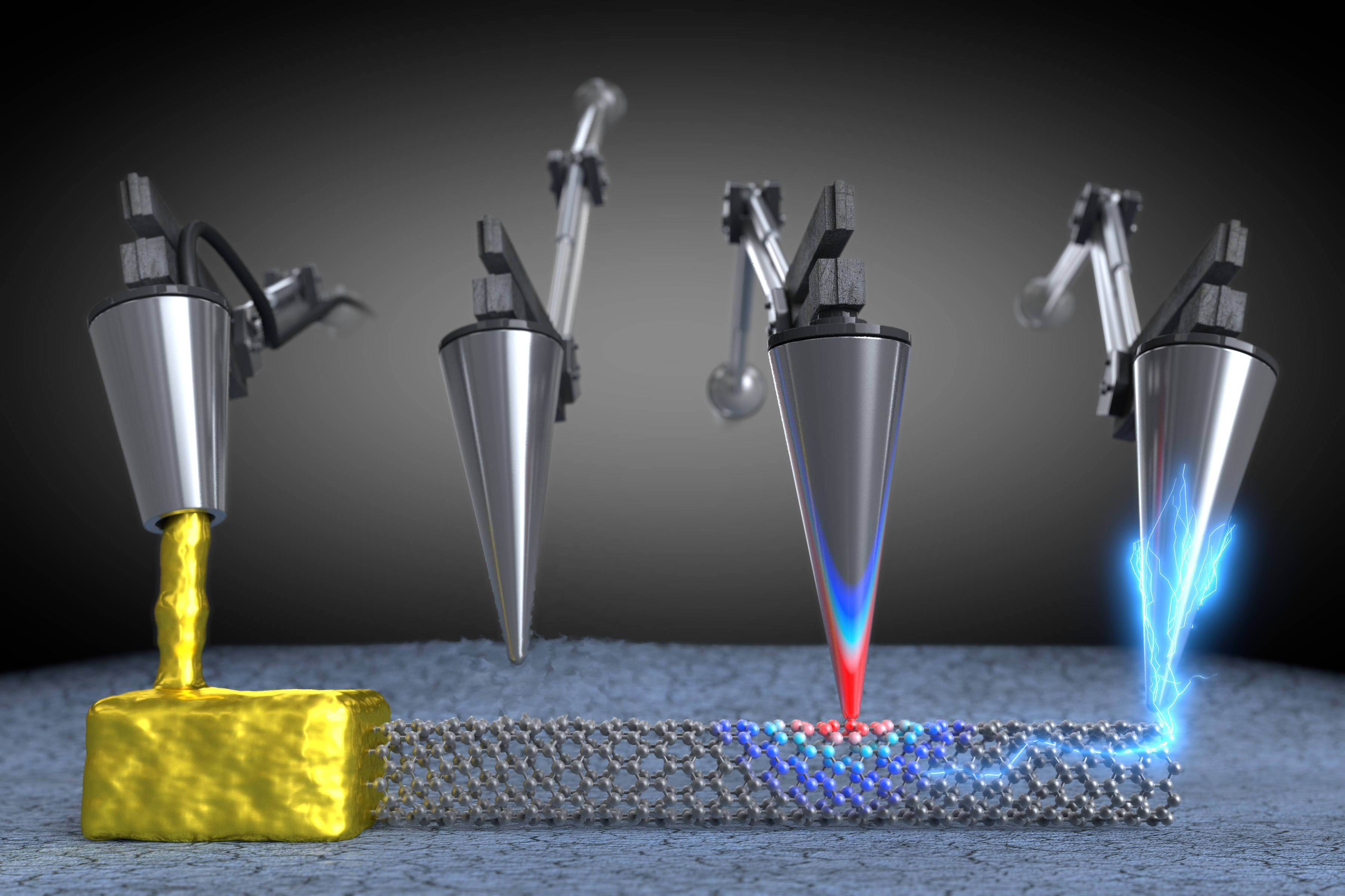
Now, the moment of combining all these techniques to carry out advanced experiments has arrived. Recently, different manufacturers have started to build prototype SPM systems provided with more than one tip in order to measure different magnitudes simultaneously. However, these machines still present many technical complications that need to be solved. For example, finding with one tip the exact location previously analyzed with another tip is extremely challenging, and avoiding collisions between the tips when placing them very near to each other is very laborious. Based on our experiences during the past 14 years, in this perspective article [23] we foresee future setups, experiments and capabilities of SPM systems, and discuss their potential impact in the future of nanoelectronics research. We propose the development of an SPM system combining multiple tips working simultaneously under a vacuum environment for advanced in situ nano-fabrication and nano-characterization (see image below). We also describe several limitations of individual techniques and propose different ways to improve their capabilities.

This perspective paper [23] is the result of hundreds of hours in front of more than 20 different SPM systems all around the world, searching for connections between different parameters and optimizing the measurements. We got confused when we found signal instabilities, felt frustrated when expensive tips broke accidentally, and got tired when the SPM session expanded until late night. But overall, we got excited when we were able to observe unique nanoelectronic phenomena, and enjoyed technical discussions with colleagues like Guenther Benstetter and Werner Frammelsberger (DIT, Germany), Oliver Krause (NanoWorld), Terry Yang (Park Systems), Louis Pacheco (CSInstruments), and David Lewis (Nanonics) among many many others, who share the passion for this amazing machine. During the past five years we have been working with different manufacturers in order to optimize their SPM systems, and we felt that sharing our vision in this perspective article could be of interest of the readership of Nature Electronics. We hope you enjoy reading it as much as we enjoyed writing it.
References
[1] G. Binnig, H. Rohrer «Scanning tunneling microscopy». IBM Journal of Research and Development 30: 4. (1986).
[2] G. Binning, C. F. Quate, Ch. Gerber, Physical Review Letters 56, 9 (1986).
[3] Murrell, M.P. et al. Spatially resolved electrical measurements of SiO2 gate oxides using atomic force microscopy. Appl. Phys. Lett. 62, 786–788 (1993).
[4] Y. Ji, C. Pan, M. Zhang, S. Long, X. Lian, F. Miao, F. Hui, Y. Shi, L. Larcher, E. Wu, M. Lanza, Boron nitride as two dimensional dielectric: Reliability and dielectric breakdown, Applied Physics Letters 2016, 108, 012905.
[5] A. Bayerl, M. Lanza, M. Porti, F. Campabadal, M. Nafría, X. Aymerich, G. Benstetter, Reliability and gate conduction variability of HfO2-based MOS devices: A combined nanoscale and device level study, Microelectronic Engineering 2011, 88, 1334.
[6] A. Bayerl, M. Lanza, L. Aguilera, M. Porti, M. Nafría, X. Aymerich, S. De Gendt, Nanoscale and device level electrical behavior of annealed ALD Hf-based gate oxide stacks grown with different precursors, Microelectronics Reliability 2013, 53, 867.
[7] K. McKenna, A. Shluger, V. Iglesias, M. Porti, M. Nafría, M. Lanza, G. Bersuker, Grain boundary mediated leakage current in polycrystalline HfO2 films, Microelectronic Engineering 2011, 88, 1272.
[8] M. Lanza, M. Porti, M. Nafria, X. Aymerich, G. Benstetter, E. Lodermeier, H. Ranzinger, G. Jaschke, S. Teichert, L. Wilde, P. Michalowski, Crystallization and silicon diffusion nanoscale effects on the electrical properties of Al2O3 based devices, Microelectronic Engineering 2009, 86, 1921.
[9] Y. Ji, J. Hu, M. Lanza, A future way of storing information: Resistive random access memory, IEEE Nanotechnology Magazine 2015, 9, 12.
[10] O. Pirrotta, L. Larcher, M. Lanza, A. Padovani, M. Porti, M. Nafría, G. Bersuker, Leakage current through the poly-crystalline HfO2: Trap densities at grains and grain boundaries, Journal of Applied Physics 2013, 114, 134503.
[11] M. Lanza, M. Porti, M. Nafría, X. Aymerich, G. Ghidini, A. Sebastiani, Trapped charge and stress induced leakage current (SILC) in tunnel SiO2 layers of de-processed MOS non-volatile memory devices observed at the nanoscale, Microelectronics Reliability 2009, 49, 1188.
[12] A. Ranjan N. Raghavan, S. J. O'Shea, S. Mei, M. Bosman, K. Shubhakar, K. L. Pey, Conductive atomic force microscope study of bipolar and threshold resistive switching in 2D hexagonal boron nitride films, Scientific Reports 2018, 8, 2854.
[13] F. M. Puglisi, L. Larcher, A. Padovani, P. Pavan, A complete statistical investigation of RTN in HfO2-based RRAM in high resistive state, IEEE Transactions on Electron Devices 2015, 62, 2606.
[14] M. Lanza, M. Porti, M. Nafria, X. Aymerich, A. Sebastiani, G. Ghidini, A. Vedda, M. Fasoli, Combined nanoscale and device-level degradation analysis of SiO2 layers of MOS nonvolatile memory devices, IEEE Transactions on Device and Materials Reliability 2009, 9, 529.
[15] V. Iglesias, M. Lanza, A. Bayerl, M. Porti, M. Nafría, X. Aymerich, L. F. Liu, J. F. Kang, G. Bersuker, K. Zhang, Z. Y. Shen, Nanoscale observations of resistive switching high and low conductivity states on TiN/HfO2/Pt structures, Microelectronics Reliability 2012, 52, 2110.
[16] N. Xiao, M. A. Villena, B. Yuan, S. Chen, B. Wang, M. Eliáš, Y. Shi, F. Hui, X. Jing, A. Scheuermann, K. Tang, P. C McIntyre, M. Lanza, Resistive random access memory cells with a bilayer TiO2/SiOX insulating stack for simultaneous filamentary and distributed resistive switching, Advanced Functional Materials 2017, 27, 1700384.
[17] Y. Shi, Y. Ji, F. Hui, V. Iglesias, M. Porti, M. Nafria, E. Miranda, G. Bersuker, M. Lanza, Elucidating the origin of resistive switching in ultrathin hafnium oxides through high spatial resolution tools, ECS Transactions 2014, 64, 19.
[18] M Lanza, U Celano, F Miao, Nanoscale characterization of resistive switching using advanced conductive atomic force microscopy based setups, Journal of Electroceramics 2017, 39, 94.
[19] M. Lanza, M. Porti, M. Nafría, X. Aymerich, E. Whittaker, B. Hamilton, UHV CAFM characterization of high-k dielectrics: effect of the technique resolution on the pre-and post-breakdown electrical measurements, Microelectronics Reliability 2010, 50, 1312.
[20] K. Tang, A. C Meng, F. Hui, Y. Shi, T. Petach, C. Hitzman, A. L. Koh, D. Goldhaber-Gordon, M. Lanza, P. C McIntyre, Distinguishing oxygen vacancy electromigration and conductive filament formation in TiO2 resistance switching using liquid electrolyte contacts, Nano letters 2017, 17, 4390.
[21] X. Lian, M. Lanza, A. Rodríguez, E. Miranda, J. Suñé, On the properties of conducting filament in ReRAM, Solid-State and Integrated Circuit Technology (ICSICT) 2014, DOI: 10.1109/ICSICT.2014.7021484.
[22] Mario Lanza, “Conductive Atomic Force Microscopy: Applications in Nanomaterials”, Publisher: Wiley-VCH, ISBN: 978-3-527-34091-0, August 2017.
[23] Fei Hui, Mario Lanza*, “Scanning probe microscopy for advanced nanoelectronics”, Nature Electronics, 2, 221-229, 2019.
Follow the Topic
-
Nature Electronics
This journal publishes both fundamental and applied research across all areas of electronics, from the study of novel phenomena and devices, to the design, construction and wider application of electronic circuits.


Please sign in or register for FREE
If you are a registered user on Research Communities by Springer Nature, please sign in