Wafer-scale integration of 2D materials in high-density memristive crossbar arrays for artificial neural networks
Published in Electrical & Electronic Engineering

In 2016, my students and I started to explore the use of hexagonal boron nitride (h-BN) as dielectric. From the very beginning, we only employed scalable methods for material synthesis and device fabrication, as we wanted that our devices could be reproduced in parallel by the industry if they exhibit any interesting performance. Therefore, we always intentionally avoided the use of mechanical exfoliation.
We started using a conductive atomic force microscope to analyze the electrical homogeneitiy and local stability of the samples [1], and found that CVD-grown h-BN is a very robust dielectric but it contains many point defects, mainly lattice distortions with a diameter of less than 1 nm [2]. Then, we fabricated 50 um x 50 um dot-like metal/h-BN/metal structures using a shadow mask and electron beam evaporator, and observed that multilayer h-BN grown by CVD is a terrible dielectric! It shows abundant leakage current, charge trapping and de-trapping and low time-to-breakdown [3]. We were very disappointed, and thought that we might need to wait many years until we can be able to grow defect-free h-BN and apply it in real devices.
However, we noticed that when electrical stresses of different polarities are applied, CVD-grown h-BN exhibits good bipolar resistive switching (RS), and that at low current limitations it also shows threshold RS [4]. We fabricated multiple devices with smaller sizes, down to 5 um x 5 um using photolithography and down to 150 nm x 150 nm using electron beam lithography, and observed that the material always exhibited stable RS. We further improved their performance to fabricate memristive electronic synapses, which showed controllable potentiation and relaxation [5].
My students and I felt very happy with these results, but we felt that something was missing. If we really wanted that our work could be useful for the industry, we really needed to demonstrate integration at the circuit level in real wafers, and report abundant information about yield and device-to-device variability.
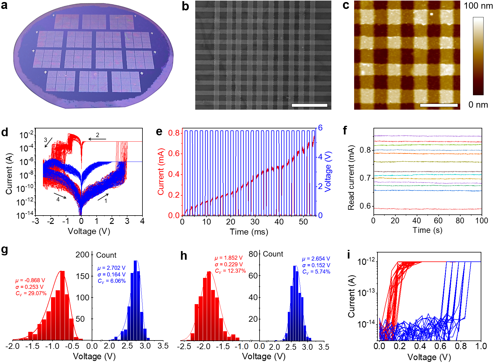
We started to fabricate many samples containing high-density crossbar arrays of memristors with sizes down to 150 nm x 150 nm in 2 inch wafers (see Figure 1). We intentionally used two types of metallic electrodes with different diffusivities, in order to try to achieve both bipolar and threshold RS. The plan worked very well, and our devices exhibited correct operation in both regimes. What we did not expect at all is that the bipolar devices would also show up to 25 stable states with linear analogue transition between them, and that the threshold devices would also exhibit stable switching with ultra-low energy consumption down to 8.8 zJ [6].
The properties of these devices were so astonishing that I could not fully trust the slides showed by my student in his weekly reports, and I decided to put three persons more to work in parallel to conduct the same experiments. We have fabricated 23 samples within a period of 18 months, using h-BN grown in different batches, and doing the lithography, metal evaporation and electrical characterization in different laboratories. All of them showed similar performance. We ended up having lot of data for multiple devices, and decided to analyze the yield and the device-to-device variability statistically. I was surprised when we realized that the yield was ~98%, and that the device-to-device variability of the switching voltages and state resistances was strikingly low (reaching an impressive value of 5.74% for the coefficient of variance of the set voltage).
I could not really believe the results I had in my hands and I decided to discuss them with two expert colleagues, Prof. Deji Akinwande and Prof. Dmitri Strukov, during the International Electron Devices Meeting held in San Francisco on December 2019. Deji gave us very useful advice on the validity of the data, the physical limits for energy consumption, and the potential reasons behind the high yield, and he shared a lot of technical knowledge regarding 2D materials integration in semiconductor lines (see for example his paper in Nature [7]). Dmitri found that our data could be very useful for the emulation of an artificial neural network, and observed that when using the data collected in our memristors the accuracy of the network for image classification was very high and the disturbance of half-selected devices was very low. Their contributions really helped to enhance the quality of our paper.
We think our work is important, not only because we report record performances, but also because we used only scalable methods and we demonstrated the performances statistically. We think our findings represent an important contribution to the integration of 2D materials in industrial production lines, which should be useful for our society.

Figure 1: a, Photograph of a two-inch wafer with Au/h-BN/Au memristive crossbar arrays distributed along it. b, SEM image of crossbar array containing 750 nm × 750 nm Ag/h-BN/Au memristors on the wafer. Scale bar, 4.5 µm. c, AFM topographic map of a part of the Ag/h-BN/Au memristor crossbar array shown in b. Scale bar, 1.5 µm. d, Representative I-V characteristics measured during 120 cycles in one single Au/h-BN/Au memristor using ICC = 1 µA (blue lines) and current compliance 1 mA (red lines). e, Sequence of PVS (5.8 V / 1 ms) showing analogue switching between two LRS shown in panel d. f, Current vs. time (I-t) curves measured at 0.1 V, showing that the conductance states during the analogue transition (panel e) are stable. g, Cumulative distribution of device set voltages and reset voltages of 48 devices using 1 mA current compliance. h, Cumulative distribution of device set voltages and reset voltages of 16 devices using 1 µA current compliance. i, Threshold-type RS characteristics of an Ag/h-BN/Ag memristor when using a current compliance 1 pA.
References
[1] Yanfeng Ji, Chengbin Pan, Meiyun Zhang, Shibing Long, Xiaojuan Lian, Feng Miao, Fei Hui, Yuanyuan Shi, Luca Larcher, Ernest Wu, Mario Lanza*, "Boron nitride as two dimensional dielectric: reliability and dielectric breakdown", Applied Physics Letters 108, 012905 (2016).
[2] Chengbin Pan, Yanfeng Ji, Na Xiao, Fei Hui, Kechao Tang, Yuzheng Guo, Xiaoming Xie, Francesco M. Puglisi, Luca Larcher, Enrique Miranda, Lanlan Jiang, Yuanyuan Shi, Ilia Valov, Paul C. McIntyre, Rainer Waser and Mario Lanza*, "Coexistence of Grain-Boundaries-Assisted Bipolar and Threshold Resistive Switching in Multilayer Hexagonal Boron Nitride", Advanced Functional Materials 1604811 (2017)
[3] Felix Palumbo, Xianhu Liang, Bin Yuan, Yuanyuan Shi, Fei Hui, Marco A. Villena, Mario Lanza*, "Bimodal dielectric breakdown in electronic devices using chemical vapor deposited hexagonal boron nitride as dielectric", Advanced Electronic Materials 1700506, 2018.
[4] Y. Shi, C. Pan, V. Chen, N. Raghavan, K. L. Pey, F. M. Puglisi, E. Pop, H.-S. P. Wong, M. Lanza*, Coexistence of volatile and non-volatile resistive switching in 2D h-BN based electronic synapses, IEEE International Electron Device Meeting, Dec. 2nd-6th 2017, San Francisco, CA, USA, DOI: 10.1109/IEDM.2017.8268333.
[5] Yuanyuan Shi, Xianhu Liang, Bin Yuan, Victoria Chen, Haitong Li, Fei Hui, Zhouchangwan Yu, Fang Yuan, Eric Pop, H.-S. Philip Wong, Mario Lanza*,”Electronic synapses made of layered two-dimensional materials“, Nature Electronics 1, 458–465 (2018).
[6] Shaochuan Chen, Mohammad Reza Mahmoodi, Yuanyuan Shi, Chandreswar Mahata, Bin Yuan, Xianhu Liang, Chao Wen, Fei Hui, Deji Akinwande, Dmitri B. Strukov, Mario Lanza, Wafer-scale integration of 2D materials in high-density memristive crossbar arrays for artificial neural networks, Nature Electronics 3, 638–645 (2020).
[7] Deji Akinwande, Cedric Huyghebaert, Ching-Hua Wang, Martha I. Serna, Stijn Goossens, Lain-Jong Li, H.-S. Philip Wong, Frank H. L. Koppens, Graphene and two-dimensional materials for silicon technology, Nature 2019, 573, 507–518 (2019).
Follow the Topic
-
Nature Electronics
This journal publishes both fundamental and applied research across all areas of electronics, from the study of novel phenomena and devices, to the design, construction and wider application of electronic circuits.


Please sign in or register for FREE
If you are a registered user on Research Communities by Springer Nature, please sign in
Mario ..it was wonderful to collaborate with you. hopefully the wafer-scalability will enable companies to consider adoption.