Light-responsive Self-Strained Organic Semiconductor for Large Flexible OFET Sensing Array
Published in Materials
Strain engineering is a fascinating physical phenomenon that is commonly found in inorganic materials and can be utilized to adjust their physical and chemical properties. But in the production process of classic inorganic semiconductors, such as silicon, germanium, the strain should be rigorously managed to assure product quality. Due to the structural differences between inorganic and organic materials, the function of strain engineering in organic semiconductors appears to receive less attention than in inorganic materials. The dilemma is gradually broken with the rapid development of flexible electronics and wearable devices, particularly for materials with photoisomerization properties. Photoisomerization typically affects the molecular arrangement of organic semiconductors, causing strain and changes in performance. However, strain engineering in small organic semiconductors has been rarely reported yet. Its mechanism is obscure, let alone the molecular engineering design that takes advantage of this phenomena.
, UV-irradiated, and Vis irradiated samples. f, Current decay fitting curve of conductive AFM. g, Time trace of IDS for the same OFET device showing the reversible photo-switching events under alternating UV and Vis irradiation.")
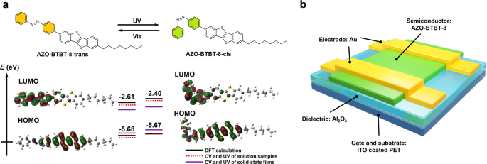
In our work, we design a photoisomerization organic semiconductor by molecule engineering, aiming to modify material properties by strain engineering. We decorated the high-performance semiconductor backbone benzo[b]benzo[4,5]thieno[2,3- d]thiophene (BTBT) with a typical photoisomerization motif-azobenzene. The alkyl chain is grafted on the other end of the BTBT to increase solubility and maintain structural balance, as shown in Fig. 1a. With AFM and UV-Vis tests (Fig. 1c and d), we discovered that the proposed AZO-BTBT-8 shows expected photoisomerization properties and the molecular packing rearrangement in the film under UV irradiation by GIXD and conductive AFM (Fig. 1e and f), which can be attributed to the strain engineering. A model for the distribution of molecular conformation and strain was proposed accordingly (Fig. 1b).
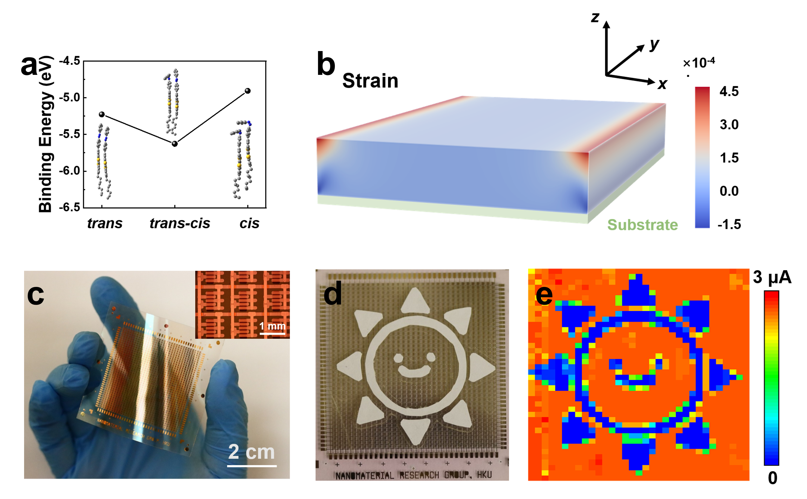
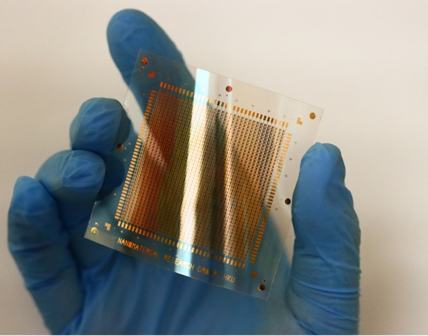
Figure 2. a, DFT molecular binding energy diagram. The insets are the corresponding packing structures. b, The calculated distributions of the strain in the long-axis direction (x-axis) in the organic film. The aspect ratio of the film section is simplified to 8000:800. Strain, the measure of the material deformation. Both stress and strain are calculated in the x dimension. c, Front-view photograph of a complete 40-by-33 OFET array on a flexible substrate. The inset shows a magnified optical image of the array. Top-view photographs (d) and corresponding current mappings (e) of a smiling cartoon sun (garland).
DFT calculations and mechanical simulations were done to support the logic of our proposed organic-semiconductor strain-engineering model (Fig. 2a and b). This photoisomerization-induced strain engineering manifests as reversible mobility improvement in OFETs, allowing us to fabricate large flexible OFET device arrays and undertake patterned sensing tests. We hope this work will provide a new perspective on molecular engineering design with target functions and the application of strain engineering in organic semiconductors.
For more details, please check out our paper “Light-responsive Self-Strained Organic Semiconductor for Large Flexible OFET Sensing Array.
Link: https://www.nature.com/articles/s41467-022-32647-9
Follow the Topic
-
Nature Communications
An open access, multidisciplinary journal dedicated to publishing high-quality research in all areas of the biological, health, physical, chemical and Earth sciences.

Related Collections
With Collections, you can get published faster and increase your visibility.
Women's Health
Publishing Model: Hybrid
Deadline: Ongoing
Tumor Microenvironment Crosstalk and Therapeutic Implications
Publishing Model: Hybrid
Deadline: Nov 02, 2026


Please sign in or register for FREE
If you are a registered user on Research Communities by Springer Nature, please sign in